Facebook
 Google
 GitHub
 Linkedin
Discrete Semiconductor Devices and Circuits
Electrical Conduction in Semiconductors
17 questions By Tony R. Kuphaldt
-
Question 4 of 17
Engineers and scientists often use energy band diagrams to graphically illustrate the energy levels of electrons in different substances. Electrons are shown as solid dots:

Based on these diagrams, answer the following questions:
- Which type of material is the best conductor of electricity, and why?
- Which type of material is the worst conductor of electricity, and why?
Reveal answer- Metals are the best conductors of electricity, because many of their electrons occupy the “conduction band” at normal temperatures.
- Insulators are the worst conductors of electricity, because a tremendous amount of energy must be invested before an electron can “leap” across the large gap into the conduction band.
Notes:I have given more information in the answer to this question than usual for me, because this subject is rather complex. One of the themes I’m trying to communicate in this question is that semiconductors are not just conductors with an unusually high amount of resistance. The mechanism of conduction in a pure semiconductor is fundamentally different from that of a metal.
Though this can become confusing, electrical conduction in metallic substances actually has two different forms: one where two electron bands overlap (permitting electrons to drift into the upper band and move between atoms), and one where the highest “unexcited” electron band is only partially filled (permitting electrons to drift into the upper regions of that same band and move between atoms). Whether or not this distinction is worthwhile to discuss in detail is a matter for you to decide.
-
Question 5 of 17
Sadly, many introductory textbooks oversimplify the definition of a semiconductor by declaring them to be substances whose atoms contain four valence-shell (outer level) electrons. Silicon and germanium are traditionally given as the two major semiconductor materials used.
However, there is more to a “semiconductor” than this simple definition. Take for instance the element carbon, which also has four valence electrons just like atoms of silicon and germanium. But not all forms of carbon are semiconducting: diamond is (at high temperatures), but graphite is not, and microscopic tubes known as “carbon nanotubes” may be made either conducting or semiconducting just by varying their diameter and “twist rate.”
Provide a more accurate definition of what makes a “semiconductor,” based on electron bands. Also, name some other semiconducting substances.
Reveal answerSemiconducting substances are defined by the size of the gap between the valence and conduction bands. In elemental substances, this definition is generally met in crystalline materials having four valence electrons. However, other materials also meet the band gap criterion and thus are also semiconductors. A few are listed here:
- Gallium arsenide (GaAs)
- Gallium nitride
- Silicon carbide
- Some plastics (!)
While Gallium Arsenide is broadly used at the time of this writing (2004), the others are mostly in developmental stages. However, some of them show great promise, especially gallium nitride and silicon carbide in applications of high power, high temperature, and/or high frequency.
Notes:I find it frustrating how many introductory electronics texts butcher the subject of semiconductor physics in an effort to “dumb it down” for technician consumption, when in fact these inaccuracies really obfuscate the subject. Furthermore, I have yet to read (October 2004) an introductory text that even bothers to mention substances other than silicon and germanium as semiconductors, despite a great deal of research and development taking place in the field of semiconductor materials
Thankfully, the internet provides a wealth of up-to-date information on the subject, much of it simple enough for beginning students to understand. This question is designed to get students researching sources other than their (poorly written) textbooks.
-
Question 6 of 17
If a pure (“intrinsic”) semiconductor material is heated, the thermal energy liberates some valence-band electrons into the conduction band. The vacancies left behind in the valence band are called holes:
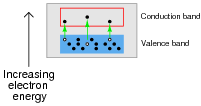
If an electrical voltage is applied across the heated semiconducting substance, with positive on the left and negative on the right, what will this do to the energy bands, and how will this affect both the electrons and the holes?

Reveal answer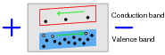
The presence of an electric field across the length of the material will cause the bands to slope, electrons moving toward the positive side and holes toward the negative.
Notes:Holes are difficult concepts to grasp for some students. An analogy I find helpful for explaining how the absence of an electron may be though of as a particle is to refer to bubbles of air in water. When viewing bubbles of air in a clear, water-filled tube, it sure seems as though the bubbles are discrete particles, even though we know them to actually be voids where there is no water. And no one balks at the idea of assigning direction and speed to bubbles, even though they are really nothing rather than something!
The principle of energy bands sloping due to the presence of an electric field is vitally important for students to understand if they are to grasp the operation of a PN junction. An analogy that helps to visualize the electron and hole motion is to think of the two bands (conduction and valence) as two different pipes that can carry water. The upper pipe (the conduction band) is mostly empty, with only droplets of water running downhill. The bottom pipe (the valence band) is mostly full of water, with air bubbles running uphill.
One major point I wish to communicate here is that “hole flow” is not just a mirror-image of electron conduction. “Hole flow” is a fundamentally different mechanism of electron motion. Electrons are the only true charge carriers in any solid material, but “holes” are commonly referred to as “carriers” because they represent an easy-to-follow marker of valence electron motion. By referring to “holes” as entities unto themselves, it better distinguishes the two forms of electron motion (conduction-band versus valence-band).
Something you might want to point out to students, if they haven’t already discovered it through their own research, is that there is no such thing as “hole flow” in metals. In metals, 100% of the conduction occurs through conduction-band electrons. This phenomenon of dual-mode electron flow only occurs when there is a band gap separating the valence and conduction bands. This is interesting to note, because many texts (even some high-level engineering textbooks!) refer to “conventional flow” current notation as “hole flow,” even when the current exists in metal wires.