Facebook
 Google
 GitHub
 Linkedin
Digital Circuits
Flip-Flop Circuits
26 questions By Tony R. Kuphaldt
-
Question 10 of 26
Plain S-R latch circuits are “set” by activating the S input and de-activating the R input. Conversely, they are “reset” by activating the R input and de-activating the S input. Gated latches and flip-flops, however, are a little more complex:

Describe what input conditions have to be present to force each of these multivibrator circuits to set and to reset.
For the S-R gated latch:
- Set by . . .
- Reset by . . .
For the S-R flip-flop:
- Set by . . .
- Reset by . . .
Reveal answerFor the S-R gated latch:
- Set by making S high, R low, and E high.
- Reset by making R high, S low, and E high.
For the S-R flip-flop:
- Set by making S high, R low, and C transition from low to high.
- Reset by making R high, S low, and C transition from low to high.
Notes:The purpose of this question is to review the definitions of “set” and “reset,” as well as to differentiate latches from flip-flops.
-
Question 11 of 26
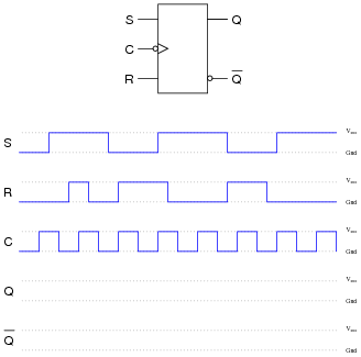
Determine the output states for this S-R flip-flop, given the pulse inputs shown:
Reveal answer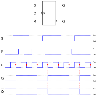
Notes:In order to successfully answer this question, students will have to identify what the “bubble” means on the clock input, and relate that to the timing diagram. Ask your students to share any tips they may have regarding the analysis of timing diagrams, specifically what points in the diagram are critical (i.e. what points in time are the only points where the outputs may actually change states).
-
Question 12 of 26
An extremely popular variation on the theme of an S-R flip-flop is the so-called J-K flip-flop circuit shown here:
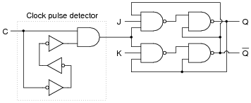
Note that an S-R flip-flop becomes a J-K flip-flop by adding another layer of feedback from the outputs back to the enabling NAND gates (which are now three-input, instead of two-input). What does this added feedback accomplish? Express your answer in the form of a truth table.
One way to consider the feedback lines going back to the first NAND gates is to regard them as extra enable lines, with the Q and [Q] outputs selectively enabling just one of those NAND gates at a time.
Reveal answer
Follow-up question: comment on the difference between this truth table, and the truth table for an S-R flip-flop. Are there any operational advantages you see to J-K flip-flops over S-R flip-flops that makes them so much more popular?
Notes:I have found that J-K flip-flop circuits are best analyzed by setting up input conditions (1’s and 0’s) on a schematic diagram, and then following all the gate output changes at the next clock pulse transition. A technique that really works well in the classroom for doing this is to project a schematic diagram on a clean whiteboard using an overhead projector or computer projector, then writing the 1 and 0 states with pen on the board. This allows you to quickly erase the 1’s and 0’s after each analysis without having to re-draw the schematic diagram. As always, I recommend you have students actually do the writing, with you taking the role of a coach, helping them rather than simply doing the thinking for them.