Facebook
 Google
 GitHub
 Linkedin
Digital Circuits
Timer Circuits
18 questions By Tony R. Kuphaldt
-
Question 1 of 18
Don’t just sit there! Build something!! Learning to analyze digital circuits requires much study and practice. Typically, students practice by working through lots of sample problems and checking their answers against those provided by the textbook or the instructor. While this is good, there is a much better way.
You will learn much more by actually building and analyzing real circuits, letting your test equipment provide the “answers” instead of a book or another person. For successful circuit-building exercises, follow these steps:
- Draw the schematic diagram for the digital circuit to be analyzed.
- Carefully build this circuit on a breadboard or other convenient medium.
- Check the accuracy of the circuit’s construction, following each wire to each connection point, and verifying these elements one-by-one on the diagram.
- Analyze the circuit, determining all output logic states for given input conditions.
- Carefully measure those logic states, to verify the accuracy of your analysis.
- If there are any errors, carefully check your circuit’s construction against the diagram, then carefully re-analyze the circuit and re-measure.
Always be sure that the power supply voltage levels are within specification for the logic circuits you plan to use. If TTL, the power supply must be a 5-volt regulated supply, adjusted to a value as close to 5.0 volts DC as possible.
One way you can save time and reduce the possibility of error is to begin with a very simple circuit and incrementally add components to increase its complexity after each analysis, rather than building a whole new circuit for each practice problem. Another time-saving technique is to re-use the same components in a variety of different circuit configurations. This way, you won’t have to measure any component’s value more than once.
Reveal answerLet the electrons themselves give you the answers to your own “practice problems”!
Notes:It has been my experience that students require much practice with circuit analysis to become proficient. To this end, instructors usually provide their students with lots of practice problems to work through, and provide answers for students to check their work against. While this approach makes students proficient in circuit theory, it fails to fully educate them.
Students don’t just need mathematical practice. They also need real, hands-on practice building circuits and using test equipment. So, I suggest the following alternative approach: students should build their own “practice problems” with real components, and try to predict the various logic states. This way, the digital theory “comes alive,” and students gain practical proficiency they wouldn’t gain merely by solving Boolean equations or simplifying Karnaugh maps.
Another reason for following this method of practice is to teach students scientific method: the process of testing a hypothesis (in this case, logic state predictions) by performing a real experiment. Students will also develop real troubleshooting skills as they occasionally make circuit construction errors.
Spend a few moments of time with your class to review some of the “rules” for building circuits before they begin. Discuss these issues with your students in the same Socratic manner you would normally discuss the worksheet questions, rather than simply telling them what they should and should not do. I never cease to be amazed at how poorly students grasp instructions when presented in a typical lecture (instructor monologue) format!
I highly recommend CMOS logic circuitry for at-home experiments, where students may not have access to a 5-volt regulated power supply. Modern CMOS circuitry is far more rugged with regard to static discharge than the first CMOS circuits, so fears of students harming these devices by not having a “proper” laboratory set up at home are largely unfounded.
A note to those instructors who may complain about the “wasted” time required to have students build real circuits instead of just mathematically analyzing theoretical circuits:
What is the purpose of students taking your course?
If your students will be working with real circuits, then they should learn on real circuits whenever possible. If your goal is to educate theoretical physicists, then stick with abstract analysis, by all means! But most of us plan for our students to do something in the real world with the education we give them. The “wasted” time spent building real circuits will pay huge dividends when it comes time for them to apply their knowledge to practical problems.
Furthermore, having students build their own practice problems teaches them how to perform primary research, thus empowering them to continue their electrical/electronics education autonomously.
In most sciences, realistic experiments are much more difficult and expensive to set up than electrical circuits. Nuclear physics, biology, geology, and chemistry professors would just love to be able to have their students apply advanced mathematics to real experiments posing no safety hazard and costing less than a textbook. They can’t, but you can. Exploit the convenience inherent to your science, and get those students of yours practicing their math on lots of real circuits!
-
Question 2 of 18
The following schematic diagram shows a timer circuit made from a UJT and an SCR:
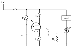
Together, the combination of R1, C1, R2, R3, and Q1 form a relaxation oscillator, which outputs a square wave signal. Explain how a square wave oscillation is able to perform a simple time-delay for the load, where the load energizes a certain time after the toggle switch is closed. Also explain the purpose of the RC network formed by C2 and R4.
Reveal answerRemember that CR1 only needs one pulse at its gate to turn (and latch) it on! C2 and R4 form a passive differentiator to condition the square wave signal from the UJT oscillator.
Follow-up question: how would you suggest we modify this circuit to make the time delay adjustable?
Notes:Knowing that the UJT forms an oscillator, it is tempting to think that the load will turn on and off repeatedly. The first sentence in the answer explains why this will not happen, though.
I got the basic idea for this circuit from the second edition of
Electronics for Industrial Electricians, by Stephen L. Herman.
-
Question 3 of 18
The model “555” integrated circuit is a very popular and useful “chip” used for timing purposes in electronic circuits. The basis for this circuit’s timing function is a resistor-capacitor (RC) network:
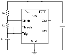
In this configuration, the “555” chip acts as an oscillator: switching back and forth between “high” (full voltage) and “low” (no voltage) output states. The time duration of one of these states is set by the charging action of the capacitor, through both resistors (R1 and R2 in series). The other state’s time duration is set by the capacitor discharging through one resistor (R2):
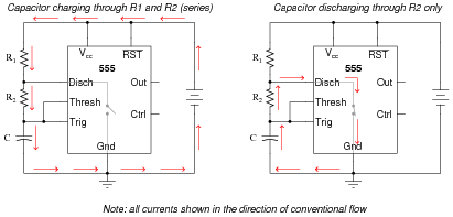
Obviously, the charging time constant must be τcharge = (R1 + R2)C, while the discharging time constant is τdischarge = R2C. In each of the states, the capacitor is either charging or discharging 50% of the way between its starting and final values (by virtue of how the 555 chip operates), so we know the expression e[(−t)/(τ)] = 0.5, or 50 percent.
Develop two equations for predicting the “charge” time and “discharge” time of this 555 timer circuit, so that anyone designing such a circuit for specific time delays will know what resistor and capacitor values to use.
Footnotes:
For those who must know why, the 555 timer in this configuration is designed to keep the capacitor voltage cycling between 1/3 of the supply voltage and 2/3 of the supply voltage. So, when the capacitor is charging from 1/3VCC to its (final) value of full supply voltage (VCC), having this charge cycle interrupted at 2/3VCC by the 555 chip constitutes charging to the half-way point, since 2/3 of half-way between 1/3 and 1. When discharging, the capacitor starts at 2/3VCC and is interrupted at 1/3VCC, which again constitutes 50% of the way from where it started to where it was (ultimately) headed
.Reveal answertcharge = − ln0.5 (R1 + R2)C tdischarge = - ln0.5 R2 C Notes:Although it may seem premature to introduce the 555 timer chip when students are just finishing their study of DC, I wanted to provide a practical application of RC circuits, and also of algebra in generating useful equations. If you deem this question too advanced for your student group, by all means skip it.
Incidentally, I simplified the diagram where I show the capacitor discharging: there is actually another current at work here. Since it wasn’t relevant to the problem, I omitted it. However, some students may be adept enough to catch the omission, so I show it here:
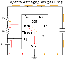
Note that this second current (through the battery) does not go anywhere near the capacitor, and so is irrelevant to the discharge cycle time.
Related Tools:
- Step-up, Step-down, and Isolation Transformers
- Design Project: Simple Component Curve-Tracer Circuit