Facebook
 Google
 GitHub
 Linkedin
A New Ratiometric Data Acquisition Circuit for Unequal Supply and Reference Voltages
This article introduces a new ratiometric data-acquisition system design for use with remote sensors. As we’ll see, it reduces error by employing matched resistor divider networks.
Ratiometric data acquisition of remote or offboard sensors is a technique that improves overall system accuracy. Designers normally think that an acquisition system ADC’s reference voltage (Vref) must be very precise. This isn’t necessarily the case in a ratiometric data-acquisition system, at least as long as the supply voltage is equal to the reference voltage (Vsupply = Vref).
However, many systems are forced to use supply voltages that aren’t equal to the reference voltage (Vsupply ≠ Vref). This can introduce a significant error into a ratiometric measurement system. This article proposes a modified system that remedies this problem, maintaining the ratiometric measurement with excellent tolerance.
A Basic Ratiometric System Review
Figure 1 shows a typical ratiometric system, in which the sensor supply voltage is equal to the Vref used to create it.
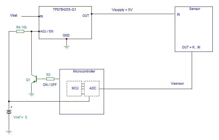
Figure 1. A ratiometric data-acquisition system where Vsupply = Vref.
The sensor outputs a voltage (Vsensor) that is proportional to Vsupply by a factor of K:
$$V_{sensor} ~=~ KV_{supply}~=~K V_{ref}$$
Equation 1.
where 0 ≤ K ≤ 1.
Vsensor is digitized by a single-ended, unipolar-input ADC having N bits and supplied with Vref:
$$ADC~output~=~\frac{V_{sensor}}{V_{ref}}(2^N~-~1)$$
Equation 2.
Because Vsupply = Vref, the resulting calculation shows that K is independent of Vsupply or Vref:
$$ADC~output~=~K\frac{V_{ref}}{V_{ref}}(2^N~-~1)~=~K(2^N~-~1)$$
Equation 3.
Tracker LDOs
Intrinsic to a ratiometric data-acquisition system is a tracker low-dropout linear regulator (LDO), which provides Vsupply. A tracker LDO differs from a standard LDO in that it doesn’t have an internal Vref. Instead, the tracker LDO output tracks an externally supplied Vref. The supply voltage to the sensor is often 5 V, which—as shown in Figure 1—then necessitates that the ADC Vref also be 5 V.
The circuit in Figure 1 uses the TPS7B4255-Q1 tracker LDO from Texas Instruments (TI), which is often used to power remote offboard sensors. It also includes features to protect against faults such as short-circuit to ground or supply, blocking of reverse current, overtemperature, and reverse polarity of supply. The tracker LDO can be disabled by pulling its ADJ/EN pin low using Q1.
Tracker LDOs do have a tracking error, which is an offset voltage (Vos) between the ADJ pin and the FB node. This output offset is 6 mV maximum for the TPS7B4255-Q1. Even in ratiometric systems like the one shown in Figure 1, Vos is not removed and remains as an error. This is because Vos changes Vsupply and therefore Vsensor, but it doesn’t change Vref. In a 5 V system, the error is only 6 mV (0.12%).
Systems Where Vsupply Doesn’t Equal Vref
As we stated previously, offboard remote sensors often have a supply voltage requirement of 5 V. In a traditional ratiometric system, this also necessitates making Vref = 5 V. However, many modern ADCs typically have a Vref of 1.8, 2.5, or 3.3 V.
If Vref and Vsupply are different voltages, then you must use resistor dividers. In Figure 2, for example, Vsupply = 5 V and Vref = 1.8 V.
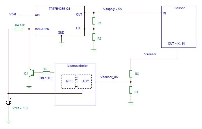
Figure 2. Schematic of a ratiometric data-acquisition system where Vsupply ≠ Vref.
A resistor divider composed of R1 and R2 in the feedback path of the Tracking LDO is used to scale Vref up to Vsupply as follows:
$$V_{supply}~=~V_{ref}\frac{R_1~+~R_2}{R_2}~=~V_{ref}(1~+~\frac{R_1}{R_2})$$
Equation 4.
Another divider must scale Vsensor down to fit within the ADC’s Vref range:
$$V_{sensor\text{_}div}~=~V_{sensor}\frac{R_4}{R_3~+~R_4}$$
Equation 5.
The resistor dividers aren’t perfect. For example, resistors with a 0.1% initial tolerance also have other error terms, as listed in Table 1. Summing all terms in Table 1 gives an absolute worst-case resistor tolerance of ± 0.65%.
Table 1. Example error terms of a 0.1% headline tolerance resistor. Data used courtesy of Texas Instruments
| Error term | Tolerance (±%) | Test conditions |
| Initial tolerance | 0.10 |
|
| Temperature drift | 0.15 | ±15 ppm/°C resistor over a 100 °C span |
| Cold temperature | 0.05 | –55 °C for 2 hours |
| Endurance | 0.10 | 70 °C for 1,000 hours of operation |
| Humidity | 0.10 | 40 °C at 93% relative humidity for 56 days |
| Temperature cycling | 0.05 | –10 °C (30 minutes) to +85°C (30 minutes) × 5 cycles |
| Vibration | 0.05 | Swept from 10 to 2,000 Hz for 7.5 hours |
| Soldering | 0.05 | 260 °C for 10 seconds |
The list in Table 1 is not exhaustive and is highly application-dependent, making the question, “What is the true accuracy of a 0.1% tolerance resistor?” surprisingly tricky to answer.
A Ratiometric Data-Acquisition System With Vsupply ≠ Vref
In Figure 2, the errors introduced into the system by the two resistor dividers aren’t cancelled. This limits the accuracy of the measurement.
One source of error is the output offset voltage of the LDO. The Vos of the tracker LDO is multiplied by (R1 + R2)/R2 and appears on the output. For example, in a system where Vsupply = 5 V and Vref = 1.8 V, the output Vos maximum is:
$$V_{os,max}~=~6~\text{mV}~\times~\frac{5~\text{V}}{1.8~\text{V}}~=~16.7~\text{mV}$$
Equation 6.
This error is divided back down again by R3 and R4 so that the Vos at the ADC is 6 mV. However, the Vref is only 1.8 V. The error from Vos at the ADC is therefore 6 mV/1.8 V = 0.33%, which is larger than when Vref was equal to 5 V.
To address this, Figure 3 shows a proposed ratiometric data-acquisition system where Vsupply ≠ Vref. In this example, Vsupply = 5 V and Vref = 1.8 V. However, this approach will also work with other common ADC reference voltages.
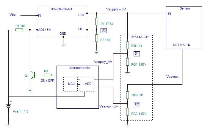
Figure 3. Schematic of proposed data-acquisition system where Vsupply ≠ Vref.
Comparing Figure 3 to Figure 2, there is now a resistor divider (D1) that scales Vsupply down so that it can also be captured by the ADC. Resistive dividers D1 and D2 are a matched pair integrated into the same package. As we’ll see later, divider D3 can be made on the OUT-to-FB of the tracker LDO using standard 1% tolerance resistors.
Using three dividers allows us to choose D3 so that it scales the 1.8 V reference voltage exactly to the 5 V supply voltage. If you were to use one of the matched pair of dividers instead, the ratios available wouldn’t allow for exact scaling of 1.8 V to 5 V. This is important because the sensor has a requirement for the accuracy of its Vsupply, and you want Vsupply to sit right at the nominal supply voltage of 5 V.
Matched Resistor Divider Networks
Figure 4 shows an example of a matched resistor divider network. The TI RES11A consists of two independent resistor dividers. The RES11A is available with different resistor divider ratios and versions qualified for automotive applications (the RES11A-Q1).
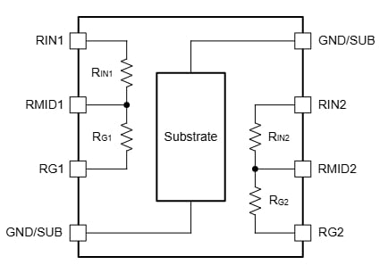
Figure 4. The RES11A or RES11A-Q1.
For all dividers, RINx = 1 kΩ. While the absolute tolerance of an individual resistor in the RES11A is quite loose (12% maximum), the fact that the four resistors are integrated into a monolithic package and are interdigitated with each other gives them excellent matching characteristics of ± 0.05% maximum.
The matching of the first divider to the second divider within the RES11A is also excellent, at ± 0.1% maximum. Furthermore, other errors, such as temperature drift, are also well matched. This results in a very low divider temperature drift of ΔtDx/ΔTa = ±2 ppm/°C drift mismatch maximum.
The resistor dividers, composed of RINx and RGx, can be connected in either direction to provide two different scaling voltages: RIN/(RIN + RG) or RG/(RIN + RG). Table 2 shows versions of the RES11A devices with different divider ratios and how each can be used to scale the 5 V Vsupply and Vsensor voltages to the target Vref voltage.
Table 2. Versions of the RES11A with different resistor divider ratios.
| Vref (V) | Device variant | Usage of RINx and RGx | Scales 5 V to … (V) |
| 1.8 | RES11A20 | RIN/(RIN + RG) | 1.67 |
| 1.8 | RES11A25 | RIN/(RIN + RG) | 1.43 |
| 2.5 | RES11A10 | RIN/(RIN + RG) | 2.5 |
| 2.5 | RES11A15 | RIN/(RIN + RG) | 2.0 |
| 3.3 | RES11A15 | RG/(RIN + RG) | 3.0 |
| 3.3 | RES11A16 | RG/(RIN + RG) | 3.12 |
The ADC that you use can be integrated into a microcontroller, as with the TI MSPM0L1306. Alternatively, it can be a stand-alone ADC such as TI’s ADS7142-Q1, ADS7138-Q1 (I2C), or ADS7038-Q1 (SPI). The ADS7142-Q1 has two input channels, while the other two ADCs have more analog inputs.
Analyzing the System’s Effectiveness
Let’s analyze the effectiveness of the measurement scheme in Figure 3. We’ll start by evaluating the resistor divider ratios (D1, D2, and D3). Dividers D1 and D2 are attenuators that scale down the voltage:
$$D_1~=~\frac{R_{IN1}}{R_{G1}~+~R_{IN1}}$$
Equation 7.
$$D_2~=~\frac{R_{IN2}}{R_{G2}~+~R_{IN2}}$$
Equation 8.
D3 is a multiplier that scales up a voltage:
$$D_3~=~\frac{R_1~+~R_2}{R_2}~=~1~+~\frac{R_1}{R_2}$$
Equation 9.
The output from the tracker LDO, including the Vos, is expressed by:
$$V_{supply}~=~D_3(V_{ref}~+~V_{os})$$
Equation 10.
Vsupply is measured by the ADC through resistor divider D1 to give Vsupply_div:
$$V_{supply \text{_} div}~=~D_1D_3(V_{ref}~+~V_{os})$$
Equation 11.
The sensor has a gain of K (0 ≤ K ≤ 1) and its output is proportional to its supply voltage. The sensor output is measured by the ADC through divider D2 as shown in Equation 12:
$$V_{sensor \text{_} div}~=~K D_2 V_{supply}~=~K D_2 D_3(V_{ref}~+~V_{os})$$
Equation 12.
The ADC has N bits and uses Vref. It performs a single-ended, unipolar measurement with an output expressed as:
$$ADC~output~=~\frac{V_{input}}{V_{ref}}(2^N~-~1)$$
Equation 13.
where Vinput is the voltage input to the ADC.
Equations 14 and 15 calculate the digitized Vsupply_div and Vsensor_div voltages as:
$$V_{supply\text{_}div\text{_}digitized}~=~D_1D_3\frac{V_{ref}~+~V_{os}}{V_{ref}}(2^N~-~1)$$
Equation 14.
$$V_{sensor\text{_}div\text{_}digitized}~=~KD_2D_3\frac{V_{ref}~+~V_{os}}{V_{ref}}(2^N~-~1)$$
Equation 15.
The microcontroller takes the digitized ADC readings of Vsupply_div_digitized and Vsensor_div_digitized and computes the ratio:
$$Computed~ratio~=~\frac{V_{sensor\text{_}div\text{_}digitized}}{V_{supply\text{_}div\text{_}digitized}}~=~K\frac{D_2}{D_1}$$
Equation 16.
The computed ratio value is independent of Vref, Vsupply, Vos, and D3. That’s why it’s possible, as we mentioned earlier, to make divider D3 using standard 1% tolerance resistors.
If the two resistor dividers in the RES11A (D1, D2) are perfectly matched, then D1 = D2 and the resulting computed ratio = K. The acquisition system is measuring only K, which is the output of the sensor from 0 to 100% of full scale.
In practice, dividers D1 and D2 are not error-free. Let’s analyze that in the next section.
Matched Resistor Divider Networks vs. Discrete Resistors
You could make dividers D1 and D2 from discrete 0.1% resistors instead of the RES11A matched resistor divider networks. However, the discrete resistors aren’t matched, and their errors don’t track each other. This would negatively impact the accuracy of the system.
Errors When Using Discrete Resistors
In any resistor divider, the tolerance of each resistor does not simply add together to create the tolerance of the divider output. The divider output tolerance also depends on the ratio of the divider (D). Equation 17 gives the relative divider error as:
$$\frac{\Delta D}{D}~=~\pm~2T(1~-~D)$$
Equation 17.
where:
ΔD is the absolute error
T is the tolerance of each resistor in the divider.
Let’s examine the limits. As D → 1, then ΔD/D → 0. As D → 0, ΔD/D → ±2T, which is the worst-case error. In other words, the higher the attenuation of the divider, the larger the error from the resistor tolerances.
By applying these results, we can evaluate the effect of using discrete resistors in the proposed system (Figure 3). We know from Equation 16 that the computed ratio from its two ADC readings is proportional to D2/D1. Equation 18 calculates the computed ratio when divider errors ΔD1 and ΔD2 are included:
$$Computed~ratio~with~error~=~\frac{D_2~+~\Delta D_2}{D_1~+~\Delta D_1}$$
Equation 18.
The resistor divider ratios are designed to be identical: D1 = D2 = D. Therefore, Equation 19 gives the error of the computed ratio as:
$$Computed~ratio~error~(\%)~=~\pm \left[\frac{1~+~2T(1~-~D)}{1~-~2T(1~-~D)}~-~1 \right]~100 \%$$
Equation 19.
As D approaches 1, the computed error ratio approaches 0. On the other hand, as D approaches 0, the computed ratio error approaches ±4T. This is the worst case.
Equation 19 also applies when considering the other errors, such as temperature drift, that we described in Table 1.
Errors When Using Matched Resistor Divider Networks
For the RES11A, the analysis is different. The matching tolerance (tM) between the two dividers has a maximum value of ±1,000 ppm, or ± 0.1%.
The temperature coefficient of each divider has a maximum value of ΔtDx/ΔTa = ±2 ppm/°C drift mismatch. Thus, a very conservative value of the temperature drift of D2/D1 is ±4 ppm/°C. The data sheet, which is linked to earlier in the article, does specify the typical matching temperature coefficient of resistance between the two dividers (ΔtM/ΔTa = ±0.05ppm/°C). However, it doesn’t give the maximum value.
Table 3 compares the errors for matched resistor divider networks with discrete 0.1% tolerance resistors. The table compares the initial accuracies and temperature drift. The use case is for the RES11A20 to make D1 and D2. For that reason, D = 0.333.
Table 3. Comparison of errors of D2/D1 when using discrete 0.1% resistors vs. the RES11A.
| Parameter | RES11A tolerance (±%) | Discrete 0.1% resistor-divider tolerance (±%) |
| Initial tolerance | 0.10 | 0.267 |
| Drift with temperature | 0.04 | 0.401 |
The total error from the RES11A is ± 0.104%, compared to ± 0.668% for the discrete resistor solution. As previously discussed, there are other error terms to consider for both cases. You can expect that the matching of the dividers in the RES11A will outperform the discrete 0.1% resistor dividers.
Simulation of the New Ratiometric Data-Acquisition System
Using the TINA-TI™ software, we’ve developed a behavioral model of the proposed ratiometric data-acquisition system. Figure 5 shows this system set up to run a DC simulation.
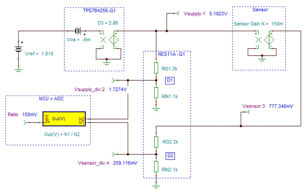
Figure 5. TINA-TI software DC analysis of a ratiometric data-acquisition system where Vsupply ≠ Vref. [click to enlarge]
The TPS7B4256-Q1 tracker LDO is modeled as a gain equal to D3. The RES11A20, with RINx = 1 kΩ and RGx = 2 kΩ, is used to scale 5 V to 1.67 V. The output of the sensor is set to K = 0.15.
To see how the system reacts in the presence of errors, D3 is increased by 3% to 2.86, Vos = –6 mV, and Vref is increased by 1% to 1.818 V. In Figure 5, the computed ratio remains at the ideal value of 0.15, which is K.
Wrapping Up
When a ratiometric data acquisition system uses a topology where Vref ≠ Vsupply, additional errors are typically introduced that impact the accuracy. We have demonstrated a new ratiometric data-acquisition system that allows these errors to be canceled.
Using a matched pair of resistor dividers such as the RES11A restores the accuracy of the acquisition system and is superior to using individual precision resistors. When compared to using 0.1% discrete resistors, the RES11A reduces the error by 6.4×.
Featured image used courtesy of Adobe Stock; all other images used courtesy of Texas Instruments
Related Content