Facebook
 Google
 GitHub
 Linkedin
PCB Stackup Basics and Using Fusion 360’s Stackup Manager
The way your PCB’s layers are arranged has huge implications for the board’s efficiency. Learn the basics of PCB stackups, and how Fusion 360’s stackup tool helps manage your PCB’s layering strategy.
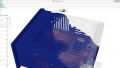
A PCB stackup refers to the arrangement of layers in a printed circuit board (PCB). The stackup plays an important role in the overall performance and reliability of the PCB. One solution to help with PCB stackups is Fusion 360, which has a layer stackup manager (Figure 1).

Figure 1. A view of Layer Stack Manager. (Click image to enlarge)
Fusion 360 allows designers the ability to specify layer thickness, materials, and many other parameters needed by PCB manufacturers and simulations. When selecting or designing a stackup, there are several factors to consider, like signal integrity (SI), trace impedance, thermal management, etc.
In this article, we’ll cover the PCB stackup basics, how the Fusion 360 stackup manager can assist in modifying your layout, and the factors you’ll need to consider when designing a stackup.
Stackup Signal Integrity: Minimizing Signal Loss and Crosstalk
To begin with, the stackup should be designed to minimize signal loss and crosstalk. The signal loss will occur on long traces, thus, it’s important tostrive to keep traces as short as possible. The dissipation factor (Df) of a substrate also plays a role in signal loss, and for very high-speed designs, it may be necessary to use a low Df substrate made of Teflon or other material.
Cross talk, on the other hand, occurs when traces couple their signal onto nearby traces. This effect can be likened to capacitive coupling, as two adjacent traces form a capacitor. A capacitor is just two conductors separated by an insulator. Keeping traces as far apart as practical will minimize crosstalk. However, it is important to remember that the coupling occurs through the electric field. For this reason, stackups ideally have a ground plane adjacent to every signal layer, as this will tightly constrain electric fields and prevent them from spreading out and interfering with other signals.
The impedance of traces will also impact SI. Mismatches cause reflections, adding noise to a signal and contributing to signal loss.
Factors That Affect the Impedance of Traces
There are several factors that can affect the impedance of traces in a printed circuit board (PCB):
Trace width:
The width of the trace affects the impedance. Wider traces have lower impedance, while narrower traces have higher impedance.
Trace Thickness:
The thickness of the trace also affects the impedance. Thicker traces have lower impedance, while thinner traces have higher impedance.
Dielectric Constant (Dk) of the Substrate Material:
The dielectric constant of the substrate material determines how far the electric field is "pushed" out of the substrate of the PCB. Materials with higher dielectric constants result in traces having lower impedances and more tightly constrained electric fields. They also tend to be more lossy.
Trace Spacing:
The spacing between the trace and any nearby conductive objects, such as other traces or planes, can affect the impedance. Closer spacing leads to higher impedance, while wider spacing leads to lower impedance.
SI Extension:
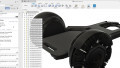
Fusion 360 Electronics has an SI extension that can calculate trace impedance for you (shown in Figure 2). This makes it easy to make changes to trace width, thickness, spacing, or Dk and quickly see how they impact impedance.

Figure 2: SI Extension showing trace impedance. (Click image to enlarge)
Trace Shape:
The shape of the trace can also affect the impedance. Straight, uniform traces exhibit constant impedances, whereas non-uniform traces will have varying impedances. These variations in impedance are called impedance discontinuities and result in signal reflections, which manifest as noise and/or loss of signal.
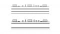
It is important to consider these factors when designing a PCB to ensure that the trace impedance is optimized for the desired performance and reliability. The Fusion 360 Electronics SI Extension enables the designer to see any impedance discontinuities, and the designer can then modify traces to minimize or eliminate them (shown in Figure 3).

Figure 3: SI Extension showing variation in impedance along a trace. (Click image to enlarge)
Fusion 360 Electronics SI Extension also allows the designer to make changes to trace widths and/or substrates to achieve the required impedances. This is especially useful for manufacturing as manufacturers will have preferred/standard stackups that differ from each other. Additionally, Fusion 360 Electronics allows for the import of preferred/standard stackups from manufacturers or others (Figure 4).

Figure 4: Layer Stack Manager showing Open Preset File. (Click image to enlarge)
Other Factors To Consider in Your Stackup
Current Carrying Capacity:
The stackup should be able to handle the current requirements of the circuit. This may involve using thicker or wider traces and planes to increase the current carrying capacity.
Thermal Management:
In PCB design, the coefficient of thermal expansion (CTE) of the materials used in the PCB is an important consideration. The CTE measures how much a material expands or contracts in response to changes in temperature.
During the manufacturing and operation of a PCB, the materials used in the PCB are subjected to temperature changes that can cause them to expand or contract. If the CTEs of the different materials used in the PCB are not well-matched, this can cause problems such as warping, cracking, or other forms of damage.
To minimize these problems, carefully select materials with CTEs that are as close as possible to one another. This can be done by selecting materials with similar CTEs or by using materials with a high CTE as a structural element and materials with a low CTE as a surface layer.
It is also important to consider the CTE of the materials used in the PCB in relation to the operating temperature range of the PCB. For example, if a PCB is designed to operate at high temperatures, it may be necessary to use materials with a higher CTE to allow for expansion without damaging the PCB.
Manufacturing Considerations:
The stackup should be designed to be easily manufacturable. Work with your PCB manufacturer and discuss with them the best stackup to achieve the impedances needed and minimize signal loss. Manufacturers will have preferred materials and thicknesses for stackups that they have perfected. Avoid non-standard layer counts or configurations.
When selecting or designing a stackup, it is important to consider the specific requirements of the circuit and the available manufacturing processes. Consult with your PCB manufacturer to ensure that the stackup is optimized for the desired performance and reliability. To ensure the fewest SI issues, ensure that your stackup uses adjacent ground planes and has impedance-controlled traces where needed with as impedance discontinuities as possible.
All images used courtesy of Autodesk