Facebook
 Google
 GitHub
 Linkedin
The Multi-Core and DSP Capabilities of the LPC5500 MCU Series
In this article, learn more about the multi-core, DSP acceleration, and co-processing features of the LPC5500 series of microcontrollers.
Arm-Cortex-M33-based MCUs offer such features as a novel coprocessor interface that can be used in embedded applications to achieve significant speed-ups.
In the Cortex-M33 architecture, the newly introduced coprocessor interface is a dedicated 64-bit interface that connects the core itself to up to eight external processing units, completely skipping the AHB bus structure. Therefore, the external processors are not subject to prioritization with other bus master devices.
Coprocessors can execute code independently of the main Cortex-M33 core, and because of that, the main CPU can send data to a coprocessor and execute other operations while it waits for the external core to finish its calculations. The Cortex-M33 core won’t stall unless it attempts to instruct a coprocessor to execute a new calculation while it’s still busy, or if it tries to read the result of a previous computation before the coprocessor is done.
In the LPC5500 MCU series, there are four coprocessors (see Figure 1 below).

Figure 1. The four coprocessors of the LPC5500 MCU series.
Two of them are FPUs and one is an additional CASPER unit that is used for accelerating security processes. However, it’s important to note that the PowerQuad unit, depicted in red, contains four single-precision floating-point multiply and accumulate units (MACs), where two are needed to perform calculations. This splits the PowerQuad into two independent units: PQ0 and PQ1. These can be utilized simultaneously for task execution.
The main CPU communicates with the coprocessors via a dedicated interface. However, the PowerQuad is also available via the AHB bus, where it acts as a slave device. This coprocessor has a private RAM interface that, together with a reserved area in the memory, can also access other parts of the RAM.
A Look Inside the PowerQuad Unit
Internally, the PowerQuad consists of the four MACs described above. Note that all the calculations are performed in floating-point data, and integers get converted automatically. Besides the interfacing controllers concerning, for example, RAM access, the PowerQuad unit contains several engines for FFT, DCT, matrix calculations, convolution, and other mathematical operations.
Utilizing the PowerQuad Unit
There are two methods for interacting with the PowerQuad: the coprocessor interface and the AHB peripheral. For simple operations, it is sufficient to use the coprocessor interface and send the opcode and operands to the unit. Examples for all supported operations in the SDK downloaded can be found in the first part of this series, The Features and Applications of LPC5500 Series Microcontrollers. With larger, more complex data structures, like matrices, this approach would quickly become very inefficient.
The PowerQuad can also act as an AHB peripheral, and it can directly access the RAM itself. Thus, more complex operations are handled by setting a series of registers, which contain pointers in the PowerQuad unit so that it can independently fetch and store the data that it needs. This is shown in the table below.
| Address | Name | Description | Access |
| 0x400A6000 | OUTBASE | Base address for the output region | R/W |
| 0x400A6004 | OUTFORMAT | Out format | R/W |
| 0x400A6008 | TMPBASE | Base address for the temporary region | R/W |
| 0x400A600C | TMPFORMAT | Temporary format | R/W |
| 0x400A6010 | INABASE | Base address for input A | R/W |
| 0x400A6014 | INAFORMAT | Input A format | R/W |
| 0x400A6018 | INBBASE | Base address for input B | R/W |
| 0x400A601C | INBFORMAT | Input B format | R/W |
The temporary region is where the PowerQuad unit will store intermediate results, the input regions contain the operands, and the output will get written to the area referenced by the OUTBASE pointer. Besides that, there are some important control registers, shown in the table below.
| Address | Name | Description | Access |
| 0x400A6100 | CONTROL | PowerQuad control access | R/W |
| 0x400A6104 | LENGTH | Length register | R/W |
| 0x400A6108 | CPPRE | Coprocessor prescale register | R/W |
| 0x400A610C | MISC | Miscellaneous use register | R/W |
The CONTROL register determines which particular calculation engine to use and is utilized for setting the opcode. It also contains various other bits, including one the user can poll to determine whether the calculation has finished. Besides these, there are a few status registers to communicate errors.
Note that some registers were omitted in this example. However, more information about these fields and their possible values can be found in NXP application notes and the official API. The document Computing FFT with PowerQuad and CMSIS-DSP on LPC5500 is also helpful, as it discusses FFTs with the PowerQuad for code examples and in-depth explanations.
If using the PowerQuad features in an MCUXpresso project is desired, it’s important to make sure PowerQuad drivers are included during creation.
A Look at the Cortex-M33 Multi-Core Capabilities
Some models of the LPC5500 series of MCUs are equipped with two Arm Cortex-M33 processing cores. The primary core, named CPU0, can utilize all features, and is always active when the MCU boots up. The second core, named CPU1, is a slimmed-down version of the primary core, and remains inactive until it is enabled by the main processing core. Both cores can access all the peripherals through the AHB bus, and they can communicate via a shared mailbox, which also provides locking mechanisms.
There are a few important registers that need to be modified to utilize CPU1 in projects. First, there are enable and reset bits in the CPU1 control register. Bits 31 to 16 must contain 0xC0C4 for changes to have an effect. Besides that, CPU0 can write the boot address of CPU1 to a register. There are some status registers for determining whether either of the CPUs is sleeping or locked up — more information about these can be found in the MCU’s user guide in section 4.5.70.

Figure 2. CPU enable and boot registers.
Chapter 52 of this same user guide also offers details about the mailbox, discussing how to assert up to 32 interrupts between the independent CPU cores and how to use the mutex register.
A Simple Multi-Core “Hello World” MCUXpresso Example
The MCUXpresso SDK for LPC55S69 comes with an example project that demonstrates the multi-core features, which can be loaded from the quickstart panel:

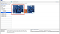
Figure 3. Select both multi-core hello world examples that come with the SDK.
Once this is done, the MCUXpresso automatically loads the linked project that will run on the secondary core. Multi-core programs are always in separate projects, making it easier to develop and debug them in different teams. The primary core must receive a compiled file and load it to a specified memory area where CPU1 will start the execution.
As explained above, CPU0 is responsible for setting up CPU1. Looking at the main c module in the core0 project, the following definition can be found:

A very early call to the multi-core manager is then shown:

This call sets up the current core and returns its number, which, in this case, is zero. Another initialization call to the multicore manager, which installs the event handlers, can be found in the main method:

A call to the multi-core manager API that initializes the second CPU core can be found towards the end of the main method:

In this example, the synchronous start option was used, which means that CPU0 will stall and wait until CPU1 is initialized and returns an event.
The project that runs on CPU1 is much simpler. It initializes the multi-core manager and then loads the startup data that got passed by CPU0 before it returns an event that releases CPU0.
To run the program, debug the CPU0 project. The MCUXpresso SDK will automatically compile it, link the associated files, and upload them to the board. The output produced by the primary project should show, and we should also be able to observe that the LED on the development board starts blinking.
NXP’s app note LPC55xx/LPC55Sxx Dual-Core Communication gives a more in-depth look at how the mailbox can be used for IPC between the two cores.
A Review of LPC5500 MCU Series
Some models of the LPC5500 MCU series come with a DSP coprocessor for fast mathematical operations. The unit is connected to the new coprocessor interface of the Arm Cortex-M33 CPU, as well as to the AHB bus.
Some simple operations can be executed solely using this new interface. Others, however, require the user to set the values of special registers. Besides this new feature, some devices from the LPC5500 series come with an additional processing core, which is a light-weight version of the main one.
There is a wealth of software examples available for the LPC5500 MCU series, based on NXP's complimentary MCUXpresso IDE and Software Development Kit (SDK). A growing list of application notes, tutorials, and videos can be found at NXP’s community page. You can also find my first-hand accounts of setting up and troubleshooting the boards, which include how-tos, deep dives, and supplemental information.