 Facebook
 Google
 GitHub
 Linkedin
Understanding and Eliminating 1/f Noise
This article defines 1/f noise and goes over ways to reduce or eliminate it in precision measurement applications.
This article defines 1/f noise and goes over ways to reduce or eliminate it in precision measurement applications. 1/f noise cannot be filtered out and can be a limit to achieving the best performance in precision measurement applications.
What is 1/f Noise?
1/f noise is low-frequency noise for which the noise power is inversely proportional to the frequency. 1/f noise has been observed not only in electronics but also in music, biology, and even economics.1 The sources of 1/f noise are still widely debated and much research is still being done in this area.2
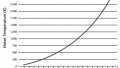
Looking at the voltage noise spectral density of the ADA4622-2 op-amp shown in Figure 1, we can see that there are two distinct regions visible in the graph. On the left-hand side of Figure 1 we can see the 1/f noise region and on the right of Figure 1, we can see the broadband noise region. The crossover point between the 1/f noise and the broadband noise is called the 1/f corner.

Figure 1. ADA4622-2 voltage noise spectral density.
How Do We Measure and Specify 1/f Noise?
After comparing the noise density graphs of a number of op-amps, it becomes apparent that the 1/f corner can vary for each product. To easily compare components we need to use the same bandwidth when measuring the noise of each component. For low-frequency voltage noise, the standard specification is 0.1 Hz to 10 Hz peak-to-peak noise. For op-amps, the 0.1 Hz to 10 Hz noise can be measured using the circuit shown in Figure 2.

Figure 2. Low-frequency noise measurement.
The op-amp is put in a unity-gain feedback configuration with the noninverting input grounded. The op-amp is powered from a split supply to allow for the input and the output to be at the ground.
The active filter block limits the bandwidth of the noise that is measured while simultaneously providing a gain of 1000 to the noise from the op-amp. This ensures that the noise from the device under test is the dominant source of noise. The offset of the op-amp is not important, as the input to the filter is ac-coupled.
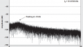
The output of the filter is connected to an oscilloscope and the peak-to-peak voltage is measured for 10 seconds to ensure we capture the full 0.1 Hz to 10 Hz bandwidth (1/10 seconds = 0.1 Hz). The results shown on the scope are then divided by the gain of 1000 to calculate the 0.1 Hz to 10 Hz noise. Figure 3 shows the 0.1 Hz to 10 Hz noise for the ADA4622-2. The ADA4622-2 has a very low, 0.1 Hz to 10 Hz noise of just 0.75 µV p-p typical.

Figure 3. 0.1 Hz to 10 Hz noise, VSY= ±15 V, G = 1000.
What Impact Does 1/f Noise Have in My Circuit?
The total noise in a system is the combined 1/f noise and broadband noise from each component in the system. Passive components have 1/f noise and current noise also has a 1/f noise component. However, for low resistances the 1/f noise and current noise are usually too small to be considered. This article will focus on voltage noise only.
To calculate the total system noise we calculate the 1/f noise and the broadband noise and then combine them. If we use the 0.1 Hz to 10 Hz noise specification to calculate the 1/f noise, then we are assuming that the 1/f corner is below 10 Hz. If the 1/f corner is above 10 Hz then we can estimate the 1/f noise using the following formula:3

where:
en1Hz is the noise density at 1 Hz,
fh is the 1/f noise corner frequency,
fl is 1/aperture time.
For example, if we want to estimate the 1/f noise for the ADA4622-2, then fh is about 60 Hz. We set fl to be equal to 1/aperture time. Aperture time is the total measurement time. If we set the aperture time or measurement time to be 10 seconds, then flis 0.1 Hz. The noise density at 1 Hz, en1Hz, is approximately 55 nV√Hz. This gives us a result of 139 nVrms between 0.1 Hz and 60 Hz. To convert this to peak-to-peak we should multiply by 6.6, which will give us approximately 0.92 µV p-p.4 This is about 23% higher than the 0.1 Hz to 10 Hz specification.
The broadband noise can be calculated using the following formula:

where:
en is the noise density at 1 kHz,
NEBW is the noise equivalent bandwidth.
The noise equivalent bandwidth takes into account the additional noise beyond the filter cutoff frequency due to the gradual roll-off of the filter. The noise equivalent bandwidth is dependent on the number of poles in the filter and the filter type. For a simple one pole, low-pass Butterworth filter, the NEBW is 1.57 × filter cutoff.
The wideband rms noise for the ADA4622-2 is just 12 nv√Hz at 1 kHz. Using a simple RC filter on the output with a cutoff frequency of 1 kHz, the wideband rms noise is approximately 475.5 nVrms and can be calculated as follows:

Note that a simple low-pass RC filter has the same transfer function as a single-pole, low-pass Butterworth filter.
To get the total noise we must add the 1/f noise and the broadband noise together. To do this we can use the root sum square method as the noise sources are uncorrelated.

Using this equation we can calculate the ADA4622-2 total rms noise with a simple 1 kHz, low-pass RC filter on the output to be 495.4 nV rms. This is just over 4% higher noise than the broadband noise alone. It’s clear from this example that 1/f noise affects systems that measure from dc up to very low bandwidth only. Once you go beyond the 1/f corner by about a decade or more, the contribution of the 1/f noise to the total noise becomes almost too small to worry about.
Since noise adds together as a root sum square, we can decide to ignore the smaller noise source if it is below about 1/5th of the larger noise source, since below a ratio of 1/5th the noise contribution is about a 1% increase in the total noise.5
How Do We Remove or Mitigate 1/f Noise?
Chopper stabilization, or chopping, is a technique to reduce amplifier offset voltage. However, since 1/f noise is near dc low-frequency noise, it is also effectively reduced by this technique. Chopper stabilization works by alternating or chopping the input signals at the input stage and then chopping the signals again at the output stage. This is the equivalent to modulation using a square wave.

Figure 4. ADA4522 architecture block diagram.
Referring to the ADA4522 architecture block diagram shown in Figure 4, the input signal is modulated to the chopping frequency at the CHOPIN stage. At the CHOPOUT stage, the input signal is synchronously demodulated back to its original frequency and simultaneously the offset and 1/f noise of the amplifier input stage are modulated to the chopping frequency. In addition to reducing the initial offset voltage, the change in offset vs. common-mode voltage is reduced, which results in very good dc linearity and a high common-mode rejection ratio (CMRR). Chopping also reduces the offset voltage drift vs. temperature. For this reason, amplifiers that use chopping are often referred to as zero-drift amplifiers. One key thing to note is that zero-drift amplifiers only remove the 1/f noise of the amplifier. Any 1/f noise from other sources, such as the sensor, will pass through unaffected.
The trade-off for using chopping is that it introduces switching artifacts into the output and increases the input bias current. Glitches and ripple are visible on the output of the amplifier when viewed on an oscilloscope and noise spikes are visible in the noise spectral density when viewed using a spectrum analyzer. The newest zero-drift amplifiers from Analog Devices—such as the ADA4522 55 V zero-drift amplifier family—use a patented offset and ripple correction loop circuit to minimize switching artifacts.6

Figure 5. Output voltage noise in the time domain.
Chopping can also be applied to instrumentation amplifiers and ADCs. Products such as the AD8237 true rail-to-rail, zero-drift instrumentation amplifier, the new AD7124-4 low noise and low power, 24-bit Σ-Δ ADC, and the recently released AD7177-2 ultralow noise, 32-bit Σ-Δ ADC, use chopping to eliminate 1/f noise and minimize drift versus temperature.
One disadvantage to using square wave modulation is that square waves contain many harmonics. Noise at each harmonic will be demodulated back to dc. If sine wave modulation is used instead, then this approach is much less susceptible to noise and can recover very small signals in the present of large noise or interference. This is the approach used by lock-in amplifiers.7

Figure 6. Measuring surface contamination with a lock-in amplifier.
In the example shown in Figure 6, the sensor output is modulated by using a sine wave to control a light source. A photodetector circuit is used to detect the signal. Once the signal passes through the signal conditioning stage it can be demodulated. The same sine wave is used to modulate and demodulate the signal. The demodulation returns the sensor output to dc, but also shifts the 1/f noise of the signal conditioning stage to the modulation frequency. The demodulation can be done in either the analog or digital domain after ADC conversion. A very narrow low-pass filter—for example, 0.01 Hz—is used to reject the noise above dc and we are left with only the original sensor output with extremely low noise. This relies on the sensor output being at exactly dc, so the precision and fidelity of the sine wave are important. This approach eliminates the 1/f noise of the signal conditioning circuitry but does not eliminate the 1/f noise of the sensor.
If a sensor requires an excitation signal, then it is possible to eliminate the 1/f noise from the sensor using ac excitation. AC excitation works by alternating the sensor excitation source to produce a square wave output from the sensor and then subtracting the output from each phase of the excitation. This approach not only allows us to eliminate the 1/f noise of the sensor but also eliminates offset drift in the sensor and eliminates unwanted parasitic thermocouple effects.8

Figure 7. AC excitation of a bridge sensor.
AC excitation can be done using discrete switches and controlling them with a microcontroller. The AD7195 low noise, low drift, 24-bit Σ-Δ ADC with internal PGA included drivers to implement ac excitation of the sensor. The ADC manages the ac excitation transparently by synchronizing the sensor excitation with the ADC conversions, making ac excitation easier to use.

Figure 8. CN-0155—Precision weigh scale design using a 24-bit Σ-Δ ADC with internal PGA and ac excitation.
Implementation
When using zero-drift amplifiers and zero-drift ADCs, it is very important to be aware of the chopping frequency of each component and the potential for intermodulation distortion (IMD) to occur. When two signals are combined the resulting waveform will contain the original two signals, as well as the sum and difference of these two signals.
For example, if we consider a simple circuit using the ADA4522-2 zero-drift amplifier and the AD7177-2 Σ-Δ ADC, the chopping frequencies of each part will mix and create sum and difference signals. The ADA4522-2 has a switching frequency of 800 kHz, while the AD7177-2 has a switching frequency of 250 kHz. The mixing of these two switching frequencies will cause additional switching artifacts at 550 kHz and 1050 kHz. In this case, the AD7177-2 maximum corner frequency of the digital filter, 2.6 kHz, is much lower than the lowest artifact and will remove all of these IMD artifacts. However, if two identical zero-drift amplifiers are used in series, the IMD created will be the difference in the internal clock frequency of the parts. This difference could be small, and therefore, the IMD would appear at much closer to dc and be more likely to fall inside the bandwidth of interest.
In any case, it is important to consider IMD when designing a system that uses zero-drift or chopped parts. It should be noted that most zero-drift amplifiers have much lower switching frequencies than the ADA4522-2. In fact, the high switching frequency is a key benefit to using the ADA4522 family when designing precision signal chains.
Conclusion
1/f noise can limit performance in any precision dc signal chain. However, it can be removed by using techniques such as chopping and ac excitation. There are some trade-offs to using these techniques, but modern amplifiers and Σ-Δ converters have addressed these issues, making zero drift products easier to use across a broader range of end applications.
References
1. W. H. Press. ‟Flicker Noises in Astronomy and Elsewhere.” Comments in Astrophysics, 1978. (PDF)
2. F.N. Hooge. ‟1/f Noise Sources.” IEEE Transactions on Electron Devices Vol. 41, 11., 1994.
3. MT-048. ‟Op Amp Noise Relationships: 1/f Noise, RMS Noise and Equivalent Noise Bandwidth.” Analog Devices, 2009. (PDF)
4. Walt Jung. ‟Op Amp Applications Handbook.” Newnes, 2005.
5. MT-047. ‟Op Amp Noise.”Analog Devices, 2009. (PDF)
6. Kusuda Wong. ‟Zero-Drift Amplifiers: Now Easy to Use in High Precision Circuits.” Analog Dialogue Vol. 49, 2015.
7. Luis Orozco. ‟Synchronous Detectors Facilitate Precision Low-Level Measurements.” Analog Dialogue Vol. 48, 2014.
8. Albert OʼGrady. ‟Transducer/Sensor Excitation and Measurement Techniques.” Analog Dialogue Vol. 34, 2000.
Related Content


can anyone tell me how to find the corner frequency of each device for analysing low frequency noise.
All graphics in the figures a gone. What happened, how can we get them back?