 Facebook
 Google
 GitHub
 Linkedin
New App Tool for Augmented Reality PCB Design Enters Beta
Ever wish you could see your design file layers overtop your spun board? Augmented reality may make that possible in real time.
Ever wish you could see your design file layers overtop your spun board? Augmented reality may make that possible in real time.
If you've ever stared at a prototype board and wondered where voltage dropoff's occurring, DebuggAR feels your pain.
DebuggAR, a San Francisco-based company, has built an augmented reality tool for PCB debugging, rework, and assembly. The mobile eCAD viewer software tool allows users to hover their phones and tablets over their PCB and instantly highlight any signals, components, and layers on the board.
The software is currently in beta, and its creators, Trevor Reeves and Mihir Shah, hope that the technology will be the lens through which EEs interact with PCBs in the future.
Augmented Reality for EEs
DebuggAR is currently an iPhone-only smartphone app tool that lets engineers and students perform component-level and net-level inspection of their designs.
The software combines the CAD information from a circuit design with a live image of a printed circuit board to let engineers isolate any number and combination of nets and components.

DebuggAR originally began as a real-time tool for design-for-assembly. Over time, the project morphed into a tool to assist with all assembly, rework, and debug through a real-time visualization of the board. The duo has assembled a small team to create an app and website that work together with Altium, Autodesk Eagle, and soon Gerbers/IPC to provide a practical augmented reality experience.
The team has only been working on the app for four months, and while the software only works with iPhone and AutoDesk Eagle / Altium at this time, the team plans to expand to other platforms in the near future.
How to Use the App
All modern-day PCBs start life as a CAD file. These CAD files describe the location, shape, layer, and net-label of each piece of copper in the board as well as the shape and position of each component. DebuggAR imports the information from the CAD files to their website where the layers are digitally reconstructed and colored. Then, the tool takes that data and combines it with a live-camera view of the board to create a virtual overlay.
Here’s the basic workflow.
1. Create a Schematic
Users create their schematic and board files in EAGLE. Alternatively, users can use one of the open-source example boards already loaded in EAGLE, like the Arduino.
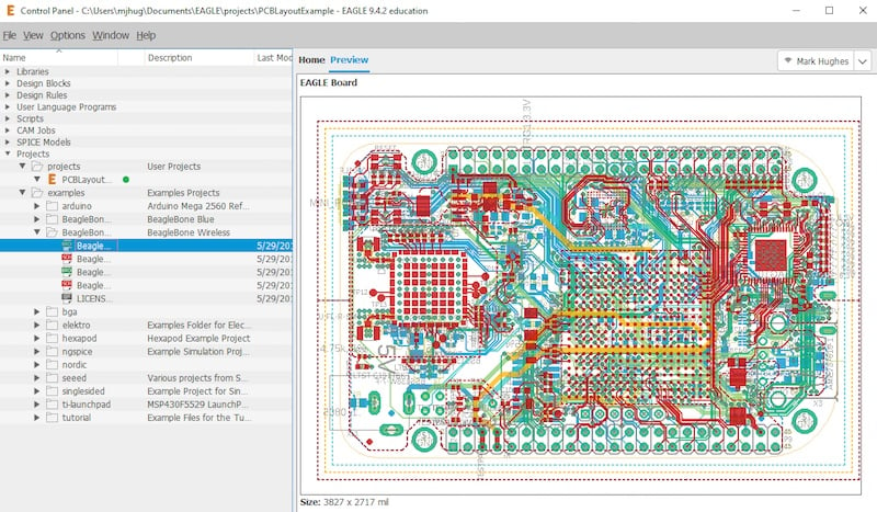
2. Upload the Schematic
Next, users upload both their EAGLE board and schematic files to the DebuggAR website. Each board is saved as a “Project.”. The software extracts part location, layers, copper nets, etc… all from the CAD file.
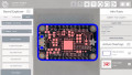
3. Take a Photo of the Board
Then, users open the iPhone app, navigate to their project, and take a photograph of their circuit board.
4. Navigate the Board Layers
It’s not terrifically useful to have all nets and layers selected as well as all components on either side of the board. Most users will select far fewer nets and components to overlay on the board.

What’s next for DebuggAR?
DebuggAR opens their platform for beta testing today. The current software requires iPhone 7 or above and iOS version 12.
Reeves and Shah have ambitious plans for the plan to expand the app to work across a wide variety of smart camera devices such as smartphones and headsets. Next on their agenda:
- Add Android & HoloLense2 support
- Increase EDA-program compatibility to include other popular programs
- Develop a video communication platform to collaborate live on debugging with remote engineers
- Support real-time collaboration between EEs anywhere in the world
Have you ever used AR on the job? What are your current methods for assessing your boards? Share your thoughts in the comments below.
Related Content


What’s this for?
Boards are so dense now we don’t put part numbers on the PCB. I assume the display can be zoomed to let us find parts on the board??