Facebook
 Google
 GitHub
 Linkedin
Evaluating the Future of 3D-Printed Integrated Circuits
A flurry of new ventures has produced powerful, silicon-on-polymer chips for complex applications—but how do they compare to standard chip designs?
Companies are Leveraging New Manufacturing Processes
ICs are typically manufactured via traditional fabrication methods, which prioritize the production of rigid devices. These rigid components are assembled in ways that protect them. According to the AFRL’s Dr. Dan Berrigan, rigidity is a handicap. It forces semiconductor manufacturers to package chips in big ways to prevent accidental damage. Internal layouts must accommodate this hardware. Unfortunately, design creativity can suffer as a result.
The push for a modern solution has gained significant steam in recent years. While there’s plenty of buzz surrounding today’s flexible ICs, memory density has held the technology back.
Traditional Meets Modern
2017 ushered in a significant leap forward in this regard. A partnership between the Air Force Research Laboratory and American Semiconductor spawned a chip “with more than 7,000 times the memory capacity of any current flexible integrated circuit on the market today.” They created the SoC to support the rise of compact consumer-and-commercial electronics.
Berrigan and American Semiconductor combined traditional knowledge with 3D printing—allowing the creation of thin semiconductor sheets with densely-packed circuitry. These ICs resemble squares of film. The printing process made it possible for researchers to integrate a compact memory controller, thus unlocking the chip’s standout performance.
A recent union between the University of Hamburg and Deutsches Elektronen-Synchrotron has facilitated 3D printing via silver nanowire meshes. These combine to form a conductive surface when bonded to a substrate. Each wire is “tens of nanometers thick and 10 to 20 micrometers long.” Polymer compression aids conductivity, and these conductive tracks are inspected using X-ray analysis. The goal is to create conductivity layers with structures resembling those of traditional ICs.
A Quick Note on Applications
In a general sense, malleable technologies like these have immense potential. 3D printing allows us to create flexible systems that act as microcontrollers. Those with integrated memory can even store sensor data, making them suitable for wearables, IoT devices, and monitoring applications.
These electronics are packed to the gills with hardware components. The ergonomic advantages let engineers optimize internal layouts—respecting form factor requirements. It’ll be interesting to see how these developments progress alongside flexible power technologies, like UMass Amherst’s Air Gen.

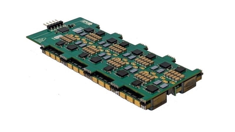
A flexible silicon-on-polymer chip developed by the U.S. Air Force and American Semiconductor. Image used courtesy of the U.S. Air Force.
Scaling Production for Mainstream Applications
3D printing’s viability will largely hinge on manufacturers’ abilities to scale or produce that technology in high yields.
Semiconductor makers are also embroiled in the nanometer race. Intel, AMD, and ARM are aiming to decrease the size of die by increasing transistor density.
These smaller designs are more capable and more energy efficient. Such attributes are crucial for smaller electronics to possess; smaller sizing promotes easier internal design, another perk of this trend. Can we chase these same improvements via 3D printing?
Evidence suggests that we have decent production bandwidth, but yields are still considered low-volume by current fabrication standards.
We can print ICs and system components directly onto PCBs, but this practice is still reasonably specialized. 3D printing owes itself to unique fabrications that don’t have widespread appeal quite yet. However, the future is very promising.
Size Considerations
The semiconductor industry currently produces numerous processes at 10nm or less. 3D printing can now achieve resolutions near the micron level only. The printing process also relies on the co-deposition of materials—certainly a technical marble, yet another complexity in the fabrication process.
Longstanding chipmaking methods employ very-large-scale integration (VLSI) to pack millions of transistors into a single chip; which is crucial for miniaturization. Since even the best 3D printers are relatively low resolution, this transistor density isn’t achievable. Improvements are needed.
Materials Advantages Paint a Promising Picture
There’s still plenty of hope for future applications. The polymers and processes involved with 3D printing have unique advantages:
-
Polymers bond well with semiconductor wafers
- Additive deposition of electrical contacts is possible via PVD, CVD, or thermal evaporation
- Polymers can handle both hot and cold temperature swings
These materials are also less fragile. 3D printed SoCs may enjoy long-term durability and performance benefits over their predecessors—especially once die sizing catches up.
What About the Costs?
Low-volume production is advantageous for 3D integrated circuits. Unlike their traditional counterparts, they don’t need to be produced on a wafer; this nullifies the cost-density issue. Manufacturing times are consistent.
The most significant determinant of price is the quantity and weight of materials used. As a result, low-volume electronics manufacturers may choose to adopt 3D printing over longstanding methods.
Should high-volume fabrication come to pass, companies must invest in new machinery. Those capital costs can add up quickly. We must also consider quality-control costs following production. It’s not unreasonable to expect kinks early on; before the manufacturing process is properly ironed out.
Forecasting the Future
3D printing may take off sooner rather than later, once the technology matures. More companies may adopt 3D printed ICs as a reliable, cheaper alternative.; which will help the technology gain visibility and momentum.
Future improvements to the printing process are necessary to vault 3D printing into the conversation. The technology produces some impressive results. Fabricators will reap the rewards once new printing technologies arise.
Related Content