 Facebook
 Google
 GitHub
 Linkedin
What is an Application-specific Integrated Circuit (ASIC)?
Indispensable for modern electrical engineering, application-specific integrated circuits (ASICs) form a diverse group of integrated circuits (ICs) that help designers to optimize sophisticated electronic devices.
There was a time when discrete components—primarily resistors, capacitors, inductors, transistors, and diodes—were sufficient for many electrical design projects. Nowadays, it’s rare to see a circuit board that doesn’t have at least one IC, and it’s not unusual to see boards that are filled with ICs of various shapes and sizes. The enormous popularity of ICs in modern electrical engineering is closely linked to the vast array of microchips that engineers can readily find, assess, purchase, and implement. However, off-the-shelf ICs sometimes don’t provide a direct path to an optimized solution, and in such cases, engineers may consider an ASIC.
What Is ASIC? Defining an Application-specific Integrated Circuit
There is no official declaration regarding the exact meaning of an ASIC, plus many electronics professionals may not always agree on what exactly an ASIC is or whether a particular component should be classified as an ASIC. Nonetheless, I think that the following definition, taken from an old issue of Analog Dialogue (p. 12), is an excellent starting point that an ASIC is:
[A]n integrated circuit designed for a specific customer, application, or market using cell-based techniques, where the necessary functional blocks are taken from a cell library, interconnected, and simulated to provide the desired system functions and level of performance. This definition excludes ICs designed with conventional “custom” design techniques.
The first part of this definition—an IC designed for a specific customer, application, or market—is a broader and perhaps more common understanding of the term. However, the second part of the definition is helpful since it distinguishes “ASIC” from simply “custom IC.” If ASIC is the same as custom IC, why do we need the term ASIC?
The full definition identifies an ASIC as an IC that offers customized functionality but doesn’t require a fully customized design process. Instead, the customized functionality is achieved through a process that is analogous to PCB design. When drawing a schematic, we take components from a library and interconnect them, and sometimes we will verify portions of the schematic via simulation. For an ASIC, designers take functional blocks from a library, interconnect them, and verify functionality and performance via simulation.
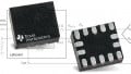
As an example, Figure 1 shows an ASIC that combines a standard digital signal processor (DSP) core with additional circuitry required for the customer’s intended application.

Figure 1. Example ASIC with a DPS. Image used courtesy of Wiki Commons and Pauli Rautakorpi [CC by 3.0]
What Does “Application Specific” Mean in ASIC?
The term “application specific" in an ASIC can be somewhat misleading. In current electrical engineering parlance, “application” usually refers to the practical purpose of electrical equipment. In other words, an electrical device’s application answers the question: what sort of useful work is this device intended to perform?
For example, in his introductory article on filters, Nick Davis explains that filter applications include radio communications, DC power supplies, and audio electronics. This means that filter circuits are useful in modules or systems whose purpose is to enable wireless communication, generate a reliable supply voltage, or reproduce high-quality sound.
It turns out that application-specific integrated circuits are often not specific to a particular application, or at least they are not limited to a particular application. A highly integrated data converter ASIC, for instance, may be designed primarily for medical imaging applications, but it is entirely possible that this same device would be similarly useful for industrial video processing or a multichannel automotive sensor network. We can even think of something more generic, such as a system-on-chip (SoC) ASIC that is initially designed for smartphones but incorporates enough functionality to be successful in a wide variety of applications.
Thus, I think that the term task-specific integrated circuit (TSIC) or functionality-specific integrated circuit (FSIC) would be more accurate. However, TSIC and FSIC definitely don’t roll off the tongue as smoothly as ASIC. In general, an ASIC is designed so that one chip can efficiently perform a specific combination of tasks. Even if this combination of tasks is initially needed for a specific application, there may be various other applications where this ASIC would be an effective and desirable alternative to off-the-shelf ICs.
The ASIC Design Cycle
Designing and verifying a customized IC, even with the help of functional blocks from a cell library, is not a trivial endeavor. If a designer can’t find the required functionality or performance among off-the-shelf ICs, the first solution is usually “keep looking.” If the difficulty persists, programmable logic—a field-programmable gate array (FPGA) or complex programmable logic device (CPLD)—may be a reasonable option.
ASIC development can require months or even years of labor and millions of dollars of non-recurring engineering (NRE) cost before a single chip has been manufactured. Thus, high-volume projects with demanding performance requirements are generally situations where management can justify the time and money involved in ASIC development. With sufficient volume, an ASIC can actually become economically advantageous. Overall production cost decreases because the decrease in component and assembly costs more than compensates for the addition of the amortized ASIC development cost. An example breakdown can be seen in Figure 3.

Figure 2. This plot compares ASIC-based development costs to programmable-logic-based development costs. As you can see, as production volume increases, the ASIC approach eventually achieves lower total production costs. Image used courtesy of Numato Lab
The list below conveys the major portions of an ASIC design project.
- System requirements and other relevant constraints are used to formulate the ASIC’s specifications.
- Specifications provide the framework for creating a high-level architectural design.
- The high-level architecture is implemented as low-level logic. As with FPGAs and CPLDs, hardware description languages (VHDL and Verilog) have become valuable tools for ASIC design.
- The design is tested to verify functionality and timing.
- The logical design must be translated into a physical layout.
- After the physical layout is verified, the project is ready for tape-out and fabrication.
- After successful fabrication and packaging, the ASIC can undergo electrical testing and be integrated into prototypes for lab and field testing.

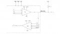
Figure 3. An example ASIC diagram. Image used courtesy of Intel
This graphic conveys the high-level architecture of an ASIC developed by Intel and Google. It’s a “programmable networking device” for “cloud and communication service providers.” See this article for more information. This is just one example of a device that has gone through the ASIC design process
All in all, ASICs are a crucial addition to high-performance and high-volume electronic devices that cannot be optimally designed using off-the-shelf components.
Have you ever been involved in ASIC development? Or do you have any personal experience with the analysis required to decide if an ASIC would be economically feasible for a certain project? Leave a comment and let us know!
Related Content


Very useful.