Facebook
 Google
 GitHub
 Linkedin
Everything Goes Up! Top Trends of 2024
Three hot technologies are leading the way in continuing the Moore’s Law performance increases that can no longer be achieved by transistor scaling alone.
In 2023, we identified AI, led by ChatGPT, as the top trend. The electronics industry put AI into everything from processors to edge IoT chips to EDA tools. If you haven’t noticed, that trend hasn’t slowed down at all.
Within our team, we discussed the major growth in electronics for automotive applications, SiC and GaN, RISC-V, quantum computing, and more. None of those would be wrong answers to the question of what was hot in 2024. But, I am choosing to highlight three often interrelated trends that exploded this past year:
- Chiplets
- Stacked high-bandwidth memory
- Photonics
How are these related, you might ask. Well, traditional Moore’s Law scaling is finally reaching physical limits. Sure, I am old enough to remember those supposed limits being discussed when transistor gate lengths were 250 nm, or 100x longer than they are today. But, this time we really mean it, probably.
Today, Moore’s Law performance increases are not driven by transistor scaling in the x- and y-dimensions. Instead, it comes primarily from these three technologies that also enable integration in the z-dimension for additional performance improvements.
So, let’s take a brief look at these hot technologies and some of our coverage from 2024. You can click on the images to read the full articles.
Chiplets
Chip designers and silicon process development engineers have long struggled with the inability to create the perfect process. One that would support high-frequency logic, high-density memories, analog circuits, high-voltage devices, efficient power routing, and more.
With chiplets, designers can mix and match different technologies while optimizing system performance, yield, and cost. In addition, as chiplets are used to enable chip stacking, additional power and performance improvements become possible. As you can see in the following articles, chip giants like AMD, Broadcom, Intel, and EDA leaders like Synopsys, Siemens, and Cadence were heavily involved in chiplet R&D.
ISSCC 2024: Inside AMD’s Zen 4c—The Area-Optimized Cloud Computing Core

The smaller size of the AMD’s Zen 4c core allows more cores per die, ultimately enhancing the performance in cloud computing applications. Image used courtesy of ISSCC and AMD
Broadcom Reaches New Processing Heights With Stacked Die and Face-to-Face Chiplets
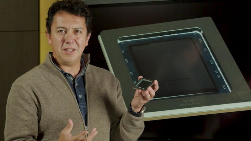
Frank Ostojic, Broadcom's general manager of ASIC products, with a 3.5D XDSiP custom accelerator chip that increases computing core area within the same overall processor package dimensions. Image used courtesy of Broadcom.
At Hot Chips, Intel Shares Details of Its Upcoming Xeon 6 SoC
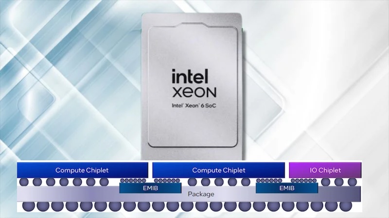
The Xeon 6 SoC uses advanced packaging technology and a chiplet architecture to minimize latency while ensuring optimal performance across the compute and I/O chiplets. Images used courtesy of Intel
Top EDA Vendors Reveal Plans to Support Intel Foundry, Including Advanced Packaging
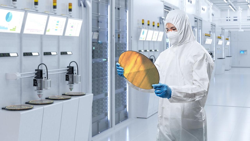
EDA vendors are enabling 3DIC developments, including chiplets. Image used courtesy of Siemens
Stacked High-Bandwidth Memory
High-bandwidth SDRAM memory, version 3E (HBM3E), is used in the highest-performance applications, including data centers, graphics, and AI. HBM3E uses a stacked die format with the CPU and HBM memory stack on the same interposer/package substrate. HBM improves performance by putting as much memory as close to the processor die as possible. Chip stacking provides Moore’s Law rate performance improvements while reducing power consumption. All the major players in the memory market had announcements in 2024 as they drive performance and chip stacks higher and higher.
Here are a few of the articles from 2024 that described this hot trend in stacked HBM.
Samsung, Micron, and SK Hynix Lead the Charge on HBM3E DRAM

Three companies—Samsung, Micron, and SK Hynix—announced moves in the high-bandwidth memory (HBM) 3E market
Memory Leaders Rise to Meet the Storage Challenges of AI
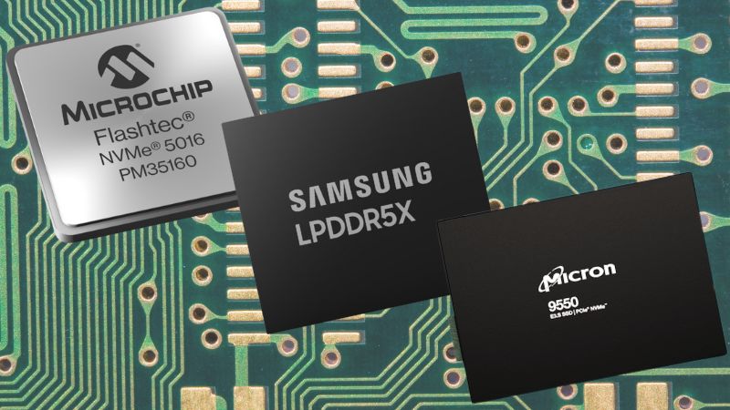
In conjunction with the 2024 Future of Memory Storage, memory makers rolled out NAND Flash, MRAM, and DDR innovations.
Density Demands Push Memory Solutions to New Heights
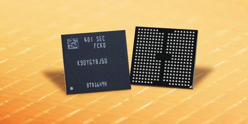
Samsung used channel hole etching technology in its new V-NAND solution, which allows holes to span a wider number of layers. Image used courtesy of Samsung
Photonics
AI models place increasing demands on computational resources and power consumption. As shown in the figure below, the energy required to train to train frontier AI models was in the hundreds of megawatt-hours for models like GPT-3. It is estimated to grow into the gigawatt-hour range for future models with trillions of parameters.

Increasing energy is required to train frontier AI models and often reaches data center capacity limits. Image used courtesy of AMD.
These increasing power requirements can be addressed by building nuclear power plants—thus, Microsoft, Google, and Meta’s investments in nuclear power to feed the AI behemoths they have created.
Perhaps a more elegant solution of interest to us at All About Circuits is to replace some of those moving electrons with photons. As the following articles describe, new photonic systems are increasingly used to increase bandwidths and decrease power consumption. Photonics also intersects with our other trends as it is integrated into chiplets and optical interposers stacked with more traditional silicon ICs.
A Q&A With GlobalFoundries’ Vikas Gupta: With Silicon Photonics, Data Centers Can Shoulder AI

GlobalFoundries representative Vikas Gupta discussed the advantages of silicon photonics for developing efficient AI chips in an All About Circuits exclusive interview. Image used courtesy of GlobalFoundries
Speeding AI Compute, Intel Debuts First Integrated Optical I/O Chiplet
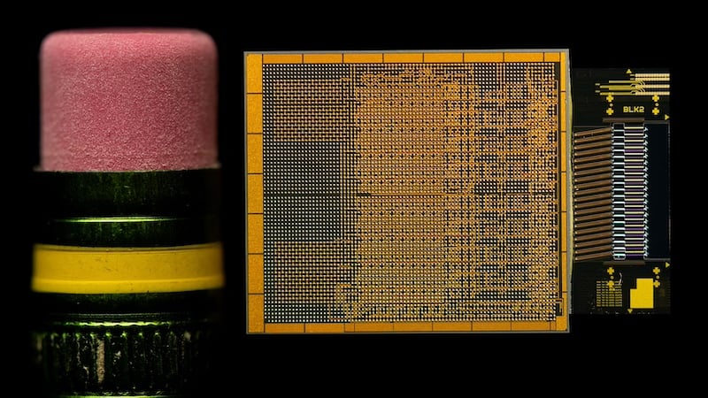
Intel believes that optical compute interconnect chiplets will "revolutionize high-speed data processing" of AI loads in data centers and high-performance computing. Image used courtesy of Intel.
Microchip and Acacia Team Up To Optimize Terabit-Scale Data Center Links
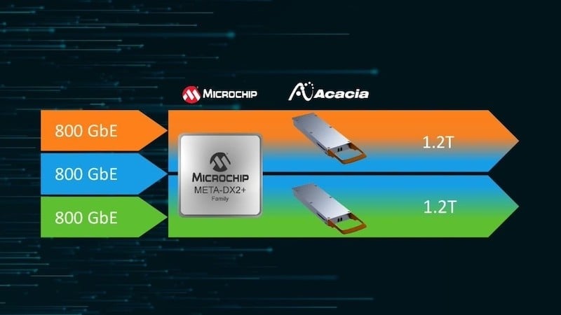
A fourth generation, terabit-scale Cloud/Data Center Interconnect (DCI) and metro transport network solution based on Microchip’s PHY and Acacia’s module. Image used courtesy of Microchip.
Can Silicon Photonics Solve the Bandwidth Bottleneck in AI Data Centers?
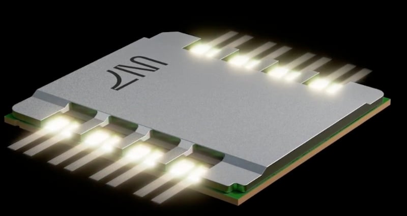
Passage is a wafer-scale, programmable photonic interconnect system for connecting arrays of heterogeneous chips. Image used courtesy of Lightmatter
Did we miss any key tech trends in 2024? Let us know the comments below so we can keep an eye on them for 2025.
Related Content