Facebook
 Google
 GitHub
 Linkedin
First PCle 6 Clock Buffers and Multiplexer “Silence” the Data Center
Locking its sights on data centers and the new PCIe Gen6 standard, Renesas has created the "industry’s first PCIe Gen6 timing solution."
Recently, Renesas released an innovative family of clock buffer and multiplexer solutions that claims to offer improved features for several applications like (IoT), machine learning (ML), cloud computing, artificial intelligence (AI), and data centers.

Renesas' latest PCIe Gen6 timing portfolio. Image used courtesy of Renesas
One highlight of this family is the low additive jitter capability of these PCIe 6-compliant solutions, which Renesas states, makes them noiseless and a good option for data center applications. With that in mind, this article explores the latest PCIe standard release, the innovative timing solutions from Renesas, and their impact on data-intensive solutions.
What is PCle 6? PCle 6 vs. PCle 3
Before delving into Renesas' new family of devices, let's take a look at PCI-SIG's recently released PCle 6 specification. This specification, which promises significant improvements to a wide range of data-intensive applications, offers advanced capabilities of this new generation allowing it to outperform the older generations, including PCle 3. The PCle 3 specification exhibits data rates of up to 8 GT/s with a 128b/130b encoding mechanism.
Moreover, PCI-SIG introduced a backchannel equalization with this generation to mitigate channel loss effects and, in addition to the encoding mechanism, the equalization allowed PCle 3 to sustain the succeeding generations of speed increases.
Overall, the PCle 3 standard also supported I/O virtualization, device sharing, and accelerator performance features such as atomics, caching hints, and transaction bypass semantics-enhancing low latency accesses. In contributing to the 2010 smartphone evolution, PCle 3 offered low-power states that enabled rapid traffic responses, fast transition times, and relatively high power efficiencies of up to 5 pJ/bit.
On the other hand, the PCle 6 specification offers data rates of up to 64 GT/s and up to 256 GB/s via x16 configuration, surpassing PCle 3 by a factor of 8. The specification utilizes the PCIe-first pulse amplitude modulation with 4 levels (PAM4) signaling and Flit (flow control unit) based encoding to offer over two times bandwidth gain.

PAM4 signaling and encoding (a) and PAM4 errors (b). Image used courtesy of PCI-SIG
The image above shows that PAM4 uses 4 voltage levels to encode 2 bits of data. Although the signaling technique exhibits a higher bit error rate (BER), it can significantly help with the channel's reach.
Moreover, unlike PCle 3, PCle 6 offers lightweight forward error correction (FEC) and cyclic redundancy check (CRC) capabilities, which significantly minimizes the BER increase associated with PAM4 signaling. While PCle 6 provides additional functionalities and simplified processing by harnessing an updated packet layout in Flit mode, it can protect customer investment and supports connections to existing products by maintaining interoperability and backward compatibility with existing PCIe technology generation.
Significance of PCle 6-compliant Clock Buffers and Multiplexers
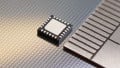
Renesas recently released PCle 6-compliant clock buffers and multiplexers to meet the rising need for high data-intensive and high-speed industrial applications such as data center/cloud computing and networking. In addition to meeting stringent PCIe 6 specifications, these new clock buffers and multiplexers provide an additional margin for PCIe 5 implementations.

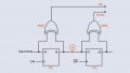
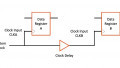
Block diagram of the RC19208A multiplexer from Renesas. Image used courtesy of Renesas
Since the PCIe 6 standard supports higher data rates of up to 64 GT/s at low clock jitter performance of at most 100 fs RMS, the standard can be useful for these latest RC190xx clock buffers and RC192xx multiplexers from Renesas.
Additionally, these PCIe 6-compliant clock buffers and multiplexers exhibit ultra-low additive jitter specs down to 4 fs RMS, which accounts for their noiselessness and create a possible option for future-proofing customer designs in light of next-gen industry standards. Moreover, PCIe 6-compliant clocks offer several low power consumption features, such as the ultra-low-power high-speed current steering logic (LP-HCSL) that replaces the conventional HCSL saving up to 85% power and multi-phase-locked loops (PLLs) with power and board-saving capabilities.
Low Additive Jitter Capability for Data Centers
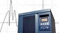
As mentioned earlier, a key feature of this family is the low additive jitter capability. Overall, jitter includes the variation or deviation from the true periodicity of a periodic signal in light of a reference clock signal. This significant factor in interconnects system design is widely undesirable because it causes display monitor flickering affects processor performance and adversely affects radio signals and transmission data losses between network devices.
A key example is the packet jitter in computer networks, which includes latency variation or the deviation from the network mean delay. The negative impact of jitters on various data-intensive applications contributes to the growing demand for low jitter components.
Thus, the ultra-low 4fs PCIe 6 additive jitter capability of this family makes the PCIe 6-compliant timing solutions a solution for data center applications. Moreover, low clock jitter performance makes these recently released solutions virtually noiseless and suitable replacements for conventional noisy data center computing components.