 Facebook
 Google
 GitHub
 Linkedin
Get Out of My Space! The Importance of PCB Keepout Areas
Learn about the concept of PCB keepout areas, why they can often be overlooked, and some tried-and-true methods for maintaining keepout areas.
Learn about the concept of PCB keepout areas, why they can often be overlooked, and some tried-and-true methods for maintaining keepout areas.
"Keepout Areas" Are Exactly What They Sound Like
A PCB "keepout area" is just as it sounds: it's an area that should be free of components and/or PCB traces.
The term component includes any electrical, mechanical, or electro-mechanical device. And, keepout areas should be maintained under all application and environmental conditions.
Now you may be thinking to yourself, "Of course! This is obvious." Many designers and engineers think the same way, and, as a result, they often trivialize the issue and then underestimate it, overlook it, or completely forget about it. This happens all too often when a specialized engineer, such as a hardware design electrical engineer, stays in his own engineering world—typically referred to as a "silo"—and doesn't consider other factors or applications for the PCB.
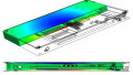
An example of an application that, perhaps, may not be considered by either a design engineer or a PCB layout person, is how the PCB may be used during board bring-up and/or troubleshooting. For instance, Figure 1 below shows a 3-pin debug header (J1) that could be used by a test engineering group for troubleshooting or updating firmware.

Figure 1. Example of an interference issue due to the lack of a PCB keepout area.
As can be seen in the figure, the header has no white outline associated with it—which typically denotes a PCB keepout area. Given the "absolute" interference issue, and perhaps the "possible" interference issues, there's no possible way—short of removing the component(s)—to attach the mating connector. This easily overlooked interference issue may result in respinning the board (and getting the wrath of management).
By comparison, Figure 2 below shows an example of a good keepout area for a slide switch. Without the white outline keepout area, it may be tempting for a PCB layout designer to place components next to the slide that would interfere with the switch when it is moved to the other position.

Figure 2. An example of a good keepout area for a slide switch.
Solving the PCB Keepout Issue: 3D Modeling
In defense of PCB layout designers, they typically use component patterns that are stored in the CAD library and are assigned to schematic symbols by the CAD librarian. In other words, PCB layout designers normally don't concern themselves with keepout areas because the PCB layout patterns should have keepout areas assigned to them, already, by the CAD librarian (we’re assuming here that the CAD librarian creates component footprints). The PCB layout designer simply grabs a PCB component/pattern, places it, and then moves on to the next component.
In my 16+ years of engineering experience, I have found two very effective methods for preventing PCB interference issues and I recommend using both methods.
The first method is to have a mechanical engineer model your design using a 3D program such as SolidWorks. The 3D model should include PCB(s), any associated enclosures, and any associated cables. If completed accurately and with enough detail, any component interference issue should be revealed early in the design phase.
When considering PCB keepout areas, one should not make the mistake of neglecting the Z-axis—that is, the area above the PCB/components. You should get in the habit of asking yourself, "Is it possible, under any realistic condition, for any object to occupy this space?"
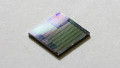
Unless you have opened up an SSD (solid-state drive), you may not realize that these memory devices use many, many electrical components that are crammed into a very low-profile area (see Figure 3).

Figure 3. Looking inside an SSD. Image courtesy of Samsung
The name of the game with SSDs, like most other commodity technology devices, is "faster, better, cheaper." Faster means faster boot-up times, as well as faster memory read and write times. Better means more memory for your computer and better energy efficiency (so your laptop or tablet can last longer on its battery charge). And cheaper means, well, less money.
In my next article, I'll go over what the "cheaper" portion of this equation means when it comes to metal enclosures. This includes my second method for preventing PCB interference issues: working closely with your teammates, including mechanical engineers. This means thinking critically about enclosure measurements and analysis, which we'll discuss further next time. See you then!
Next Article: Get Out of My Space! PCB Keepout Areas in the Z-Axis


we can build board as you want ,, as your gerber.
Br
Steven