Facebook
 Google
 GitHub
 Linkedin
Image Sensor Roundup: Toshiba, Sony, and Samsung Zero In on Industrial and Smartphone Applications
These new devices are forging innovation in image sensor technology—speeding up industrial equipment, doubling up on pixels, and capturing both visible and invisible light.
Multiple companies have brought cutting-edge image sensors to the market recently, including Toshiba, Sony, and Samsung. These image sensors have the ability to enhance the image processing systems that they will be placed within, each because of their own unique innovations.
A Brief Review of Image Sensor Technology
Before we dive into the nitty-gritty of these sensors, it's important for us to first establish what an image sensor is.
In short, an image sensor takes light as an input and converts it to an electrical signal. The image sensor then takes the parameters of the light it receives, such as color and brightness, and passes that through the processing circuitry to be turned into an image that we can see.
Photodiodes are the component of choice to do this work, and a photodiode is a PN junction. When it is struck by incident light, it begins to produce electron-hole pairs and thus conducts current, as shown in the diagram:

Photodiodes schematic symbol and cross-section. Image used courtesy of Robert Keim
These make up the pixels within image sensors, which make up the images we see. The light of each pixel is grouped to produce a whole image.
So, overall an image sensor is a collection of photodiodes that collect light and turn it into an electrical signal that is then sent to processing circuitry to obtain the captured image. For more in-depth information on this circuitry, check out AAC contributor Robert Keim's entire technical article series on the ins and outs of image sensors.
To get a brief glimpse at how image sensor technology is developing around the industry, let's review each of the new devices from Toshiba, Sony, and Samsung—highlighting noteworthy specs and the problems they aim to solve.
Toshiba's Sensor to Speed Up Industrial Equipment
Toshiba has recently launched two new image sensors, the TCD1105GFG and the TCD1106GFG. These sensors are lens reduction type (lens is curved to reduce component complexity), 1500-pixel monochrome CCD linear image sensors.
CCD, which stands for charge-coupled device, refers to the circuit topology. CCD is an analog design that optimizes noise and pixel-uniformity but requires a myriad of voltage sources to run properly.

Block diagram of the TCD1105GFG. Image used courtesy of Toshiba (PDF)
These image sensors are designed to speed up industrial equipment that requires sensors while consuming little power. The device has a maximum data rate of 25 MHz and (surprisingly for a CCD system) a single 3.3 V power supply.
They also contain internal control circuitry, such as a sample and hold circuit and timing generator, which minimizes the components needed alongside it.
The TCD1105GFG contains an internal shutter function. On top of all this, it has a pixel size of 5 μm by 50 μm. These larger pixels will take in more light, thus increasing the light sensitivity of this sensor.
Samsung Combines Four Pixels in One for Smartphones
In recent weeks, Samsung has also released its own image sensor to make its presence in the smartphone camera industry.
The ISOCELL GN1 is a 50MP sensor with 1.2 μm-sized pixels. These small pixel sizes increase the precision and detail of the produced image.
However, the size also increases light sensitivity by grouping four pixels of the same color filtering right next to each other—differing from the nominal RGB method where three LEDs of different colors are put next to one another.
This will allow four pixels to act as one larger one, and thus increase light sensitivity, giving optimal imaging in low-light conditions.

Samsung says the ISOCELL GN1 delivers more precise images, even in shadows, mid-tones, and highlights. Image used courtesy of Samsung
The sensor is able to actively and precisely focus on objects by using a photodiode pair for a pixel, and the image sensor will continue to adjust until the two photodiodes have the exact same response—meaning they are focused on the same exact object.
This technology is usually utilized in smartphone cameras for up to 10% of its pixels. But now, Samsung has developed all of its pixels using this technology.
The sensor gives the four mini-pixels that make up a single pixel different exposure times, which will allow them to detect shadows and other details better, thus producing high-quality images in areas with varying amounts of light.
Sony Sensors Sense SWIR and Visible Light
Sony's claim to fame in image sensors is the ability to sense short-wavelength infrared (SWIR) light as well as visible light. Specifically, the new Sony image sensors can sense light with wavelengths ranging from 0.4 μm to 1.7 μm.
They do this with a novel microelectronics design technique where they use a copper-to-copper connection between the compound making up the photodiodes and the silicon layer. This is where the readout circuitry is located.
While multiple cameras are usually needed to take images through this large wavelength range, Sony's new sensors can make do with a single camera.

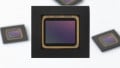
IMX990 SWIR image sensor. Image used courtesy of Sony
The two sensors, the IMX990 and IMX991, are 8.2 mm and 4.1 mm in diagonal size with 1.34MP and 0.34MP respectively. Both sensors contain thermoelectric cooling devices built into the package, minimizing the size of the chip. Sony says the sensor contains the industry’s smallest 5 μm pixels for SWIR image sensors.
These sensors also support digital output, performing similarly to industrial CMOS image sensors, according to Sony. They include many of the normally external circuits required by image processing systems, which, in turn, cuts cost, footprint, and overall power consumption of the total system.
Conclusion
Each of these devices demonstrates how image sensors are advancing in manifold ways—whether they improve the performance of industrial equipment, provide stellar smartphone images, or take precise images over a broad range of visible and invisible light.
While it’s difficult to provide a one-to-one comparison of these sensors because of their vastly different uses, they do represent the flexibility of this technology. For instance, the Sony sensor utilizes novel design methodologies on a small scale, while Toshiba has optimized CCD circuit topology by only requiring a single power supply.
Do you work directly with image sensors? In what ways have you seen this technology advance in recent years? Share your experience in the comments below.