
 Facebook
 Google
 GitHub
 Linkedin
It Was Technology Innovation Galore at Embedded World 2025
Enjoy this fresh crop of technology news from the Embedded World 2025 trade show in Nuremberg, Germany.
We had an amazing week at the Embedded World 2025 show in Nuremberg, Germany. The All About Circuits and EETech team enjoyed a very productive mix of scheduled meetings and impromptu drop-bys. We witnessed an impressive variety of embedded technologies and products, and had tons of great conversations. To give you a glimpse, in this newsletter, we’ve rounded up the highlights from a handful of the many companies that had news to share at the show.
My personal thanks to every company and every person we interacted with, whether it was talking with us, letting us take cool pics, or just making a connection. See you next time. I can’t wait!
- Jeff Child, Editor-in-Chief for All About Circuits
Altera Releases New FPGAs for Smart Edge Devices
At the show, Altera announced new FPGAs that designers can leverage to bring higher integration and performance to future edge devices.
For IoT system designs, which require highly distributed computing capabilities, designers are often left with a tradeoff between size and performance. Altera hopes to alleviate this tradeoff with its new Agilex 3 series of FPGAs and allow designers to continue innovating in a wide spectrum of industries.
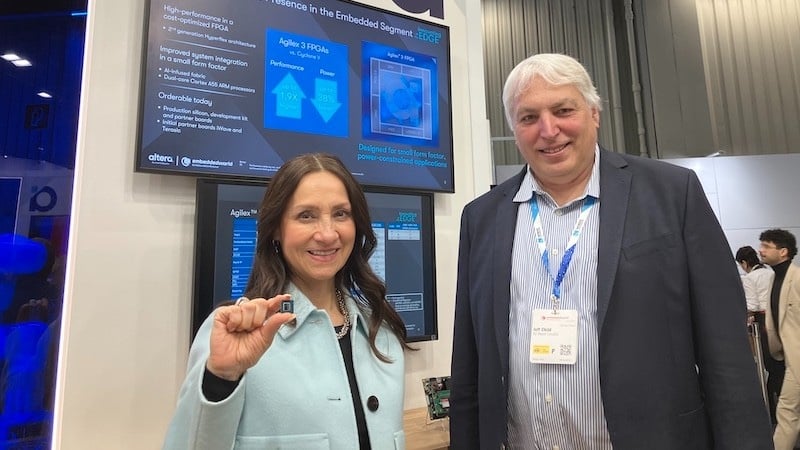
Altera CEO Sandra Rivera holding an Agilex 3 FPGA (left), All About Circuits editor Jeff Child (right).
To learn more about the Agilex 3 series of FPGAs, All About Circuits joined a pre-briefing with Sandra Rivera, CEO of Altera. Jeff Child also had a chance to meet with Rivera at the show (see image above), and learn more about what’s happening at Altera.
To address the need for better computation in edge devices, Altera’s new Agilex 3 series of FPGAs provides designers with more logic density at lower powers. Compared to previous generations of Agilex FPGAs, the Agilex 3 series sports up to 1.9× higher performance with 38% lower power, greatly reducing the struggle to integrate high-performance logic in edge devices.
We asked Rivera what her perspective is on the age old question of FPGAs vs. ASICs. “It turns out for many applications, it isn't always an either/or [between ASICs and FPGAs]—it's and,” Rivera explained. “Content expected to change over time can run on an FPGA while content (workloads and algorithms) you're confident is hardened can run on an ASIC.”
Agilex 3 FPGAs are available now, along with developer kits, partner boards, and system-on-modules.
NXP Rolls Out Automotive MCU for Zonal SDVs, Leveraging MRAM
At Embedded World, NXP Semiconductors unveiled the S32K5, a new microcontroller family designed to accelerate the transition to zonal architectures in automotive design. NXP claims the S32K5 as the industry’s first automotive MCU that is built on a 16 nm FinFET process and integrates embedded magnetic RAM (MRAM) in place of conventional embedded flash storage.
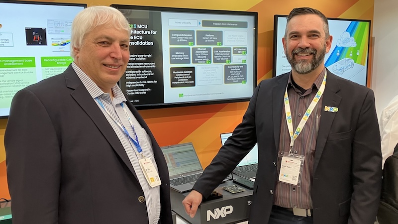
Jeff at NXPs Embedded World booth with David Vieira, Zonal Segment Lead for Automotive, learning about NXPs new S32K5 automotive microcontroller.
For the article, we spoke with David Vieira (in image above), Zonal Segment Lead for Automotive at NXP. “These are high-performance, low-latency real-time computing control MCUs,” says Viera, “We’re addressing zonal architectures as well as X-in-1 electrification use cases. This MCU family is really designed to enable a smooth transition from distributed ECUs to a zonal model.”
NXP is doing this by making the S32K5 an extension of its CoreRide platform so that automakers can scale their software-defined vehicle (SDV) architectures with pre-integrated software and reference solutions. The MCU features Arm Cortex-R52 and Cortex-M7 cores running at up to 800 MHz, an integrated 2.5 Gbps Ethernet switch, CAN-XL support, and a post-quantum cryptography (PQC)-ready security engine.
One of the most significant architectural changes in the S32K5 is the use of embedded MRAM instead of traditional embedded flash. MRAM offers a write speed of nearly 8.8 MB per second, which significantly surpasses conventional embedded flash technologies. This improvement directly benefits over-the-air (OTA) update performance by reducing the time required to reprogram ECUs both in manufacturing and in the field.
Texas Instruments Debuts ‘World’s Smallest’ MCU at Embedded World
At its Embedded World press conference, Texas Instruments released what it claims is the "world's smallest MCU" at 1.6 mm x 0.861 mm, or roughly the size of a 0603 passive component.
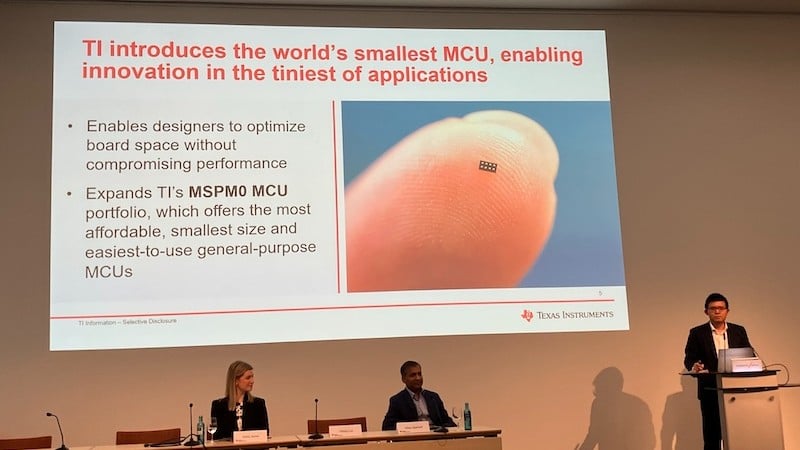
At its Embedded World press conference, Texas Instruments unveiled the MSPM0C1104YCJR Arm Cortex M0+ 32-bit MCU.
The MSPM0C1104 MCU comes in multiple chip packages, with the smallest coming in an eight-bump ball grid array (BGA) wafer-level chip-scale package (WCSP) that is 38% smaller than the next smallest competitive MCU. The MCU can operate in run mode as low as 87 µA/MHz and hold a shutdown mode at 200 nA for compatibility with micro-sized wearable devices.
The MCU has a 32-bit Arm Cortex M0+ core clocked at 24 MHz frequencies. For memory, the device supports either 8 KB or 16 KB of Flash and 1 KB of SRAM. It accepts supply voltage from 1.62 V to 3.6 V and has two 5 V tolerant open drain peripheral pins. It features an internal 24 MHz oscillator with an accuracy from -2% to +1.2% to support a minimal set of external components.
It comes in seven packages ranging in size from a 20-pin TSSOP with 18 GPIOs down to an 8-pin WCSP with 6 I/O pins. The smallest incarnation, the YCJ variant, takes up just 1.3776 mm² in area, about the size of a flake of pepper. It has eight BGA bumps with six pins for GPIO.
Synaptics Intros Multimodal Edge AI MCU and Triple Combo Wireless SoC
At the show, Synaptics had two major releases: an expansion of their SR Series of multimodal edge AI MCUs and the new SYN461x family of wireless SoCs.
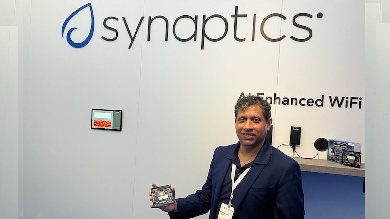
At the show, Synaptics' Ananda Roy shows us the SYN461x in action.
The Synaptics SR Series, which consists of the SR110, SR105, and SR102, seeks to integrate high-performance edge computing with multimodal AI processing in a way that optimizes power efficiency for IoT applications.
All three devices are built on the Arm Cortex-M55 architecture with Helium technology, with the SR110 and SR105 adding an Arm Ethos-U55 NPU to support intelligent, always-on sensing and scalable inference capabilities. The series includes multiple operational tiers: high-performance (100 GOPS), efficiency, and ultra-low-power (ULP) always-on sensing, allowing adaptive workload execution based on system demands.
Meanwhile, the Synaptics SYN461x is an ultra-low-power wireless SoC designed for embedded Edge AI IoT applications. Fabricated using a 22 nm process node, it integrates Wi-Fi 6E, Bluetooth 6.0, and IEEE 802.15.4 (Zigbee/Thread), making it a “triple-combo connectivity solution”.
To this end, the SoC delivers a peak data rate of 50 Mbps while maintaining low power consumption, with active transmit at approximately 300 mA and active receive at around 30 mA. Meanwhile, sleep currents can be even lower than 100 µA.
The SoC also incorporates separate processor cores for Wi-Fi and Bluetooth functions and host CPU offloading, utilizing an Arm Cortex-R4 for Wi-Fi and a Cortex-M4 for Bluetooth. Additionally, Bluetooth 6.0 support includes advanced features such as Channel Sounding for distance measurement and LE Audio with Auracast broadcast capabilities.
AMD Shakes Up Chip Architecture In New Server-Grade Embedded Processors
At Embedded World, AMD announced its latest 5th Gen EPYC embedded processors, the AMD EPYC Embedded 9005 Series (also called "Embedded Turin"). These processors leverage AMD's advanced "Zen 5" and "Zen 5c" architectures to confront rising demands driven by artificial intelligence workloads and substantial data storage growth.
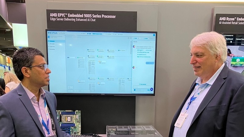
At the show, an AMD representative showed Jeff Child AMD’s demo for its newly announced Embedded 9005 Turin processor.
One of the primary improvements in this new processor is its use of TSMC’s 3 nm and 4 nm process nodes to enhance power efficiency and transistor density over the previous 5 nm, Genoa-based architecture. With greater density, the series scales from 8 to 192 cores across 17 different SKUs.
Each processor integrates Zen 5 and Zen 5c cores. Zen 5 delivers higher single-threaded performance, while Zen 5c focuses on maximizing core density within a given power envelope. With an increased L3 cache of up to 512 MB, DDR5-6400 memory support, and a memory bandwidth of 614 GB/s, the platform is said to significantly improve throughput for storage controllers, industrial automation, and AI-driven networking workloads. AMD has optimized the Embedded Turin processors for PCIe Gen 5 connectivity, with up to 128 PCIe lanes in a single-socket configuration and 160 lanes in dual-socket setups.
Unlike AMD’s EPYC processors for data centers, the Embedded 9005 Series incorporates features specifically tailored for embedded applications. These enhancements largely focus on platform longevity, system resiliency, and secure boot mechanisms.
For longevity, AMD guarantees a seven-year product availability window that extends lifecycle stability for OEMs who require long-term deployments. The silicon is also characterized for extended operating temperatures, functioning reliably between -5°C and 60°C.
For more on AMD’s Embedded World presence, check out All About Circuits' exclusive interview with AMD VP Kirk Saban.
ADI Expands CodeFusion Studio Toolset for Data Security and More
At the show, Analog Devices unveiled the latest expansion to its CodeFusion Studio to simplify the development of complex processing systems. Initially launched in October 2024, CodeFusion Studio connects code to hardware using a graphical interface. This expansion includes several new features and offerings, all of which aim to provide a more intuitive view of system functionality and data fidelity.

At Embedded World 2025, Kevin Townsend, System Planner Engineer at Analog Devices, showed us the details of the CodeFusion new capabilities.
One of the key new features in CodeFusion Studio is the System Planner, which displays resource consumption, configuration, and core-level processing. While single-core architectures are still commonplace for a variety of applications, modern innovations can often demand multiple unique cores, creating new hurdles when developing software.
Analog says CodeFusion Studio's System Planner gives designers a new way to heterogeneously integrate multiple cores in a simple, intuitive fashion. Within the System Planner, designers will find a bounty of resources that can simplify the development process from graphical resource allocation to multi-core project creation.
Analog has also introduced its Data Provenance solution that enhances data trust in edge devices. In the IoT, where devices are widely distributed and more subject to malicious activity, data trust is critical to ensure proper functionality. The Data Provenance solution may help designers maintain a robust level of security in their data.
The System Planner and Data Provenance solution will be available for download on April 25 of this year, along with early access kits and support through the ADI Developer Portal.
EW 25 Quick Briefs
-
Microchip launched its PIC32A family of 32-bit MCUs. The 200 MHz devices integrate up to 40 Msps 12-bit ADCs, high-speed 5 ns comparators and 100 MHz Gain Bandwidth Product (GBWP) op amps for intelligent edge sensing.
-
Silicon Labs unveiled its new Series 2 BG29 family of wireless SoCs. The device is well suited for intensive Bluetooth LE applications like wearable health and medical devices, asset trackers, and battery-powered sensors.
-
Morse Micro introduced the MM8102 Wi-Fi HaLow SoC, a low-power, long-range wireless solution optimized for IoT deployments in Europe and the Middle East. The SoC operates in the sub-GHz ISM band.
-
LDRA announced that the LDRA tool suite now supports the hardware-based, multicore mitigation capabilities of RISC-V processors. This includes analyzing the impact of shared resources and data coherency on worst-case execution time (WCET).
-
Renesas unwrapped its new RZ/V2N MPU that comes with firm’s proprietary AI accelerator, DRP (Dynamically Reconfigurable Processor)-AI3, boasting 10 TOPS/W power efficiency and an AI inference performance of up to 15 TOPS.
Featured image used courtesy of Embedded World. All other images taken by All About Circuits at Embedded World 2025.









Zonal SDVs: no more than distributed processing NO?