 Facebook
 Google
 GitHub
 Linkedin
New GaN Transistor Combines Si Gate Driver in Same Package
In an attempt to create smaller and more efficient charging solutions, STMicroelectronics has combined GaN transistors in the same package as gate drivers.
In recent years, gallium nitride (GaN) power transistors have gained popularity in the power electronics industry. As the demand for GaN transistors has grown, engineers have been looking for ways to create an easy drop-in replacement for Si MOSFETs with GaN transistors to simplify integration.

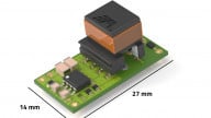
GaN transistor layout. Image used courtesy of the MIT Energy Initiative
Unfortunately, this has posed serious challenges. Initial attempts to create drop-in replacements resulted in either no significant performance improvement or even degradation in some situations.
Researchers attribute this to the fact that GaN power devices require different gate driving techniques and were not being driven properly to fully exploit their true performance. As such, the development of GaN gate drivers has been an area of interest for researchers and design engineers alike.
Gallium Nitride Transistors: An Overview
To understand why GaN transistors require unique driving techniques, we must first discuss the device characteristics.
A GaN transistor utilizes gallium nitride as the substrate as opposed to silicon in conventional transistors. An important feature of GaN is that it offers extremely high electron mobility compared to silicon, allowing it to have a high critical electric field.
Because of their higher electron mobility, GaN devices are smaller in size for a given on-resistance (or a smaller on-resistance for the same size) and feature a high breakdown voltage.

GaN vs. Si transistors. Image used courtesy of EPC
The higher electron mobility and smaller size also make GaN transistors significantly faster than traditional MOSFETs. GaN transistors offer a much lower figure of merit due to lower on-resistance and gate charge QG compared to its silicon counterparts.
Finally, GaN transistors do not suffer from a strong negative temperature coefficient like MOSFETs.
All of these features combine to create unique drive requirements for GaN FETs. It is also worth noting that most GaN devices are intrinsically depletion-mode devices, meaning that their channel is on until presented with a positive VSG.
Driving a GaN FET
For a cascode (half-bridge) GaN configuration, which is a standard topology, the gate driver can be similar to those for a power BJT or MOSFET. However, the challenge is the need for high-frequency capability (in the order of several to tens of MHz). At a given level of gate drive power loss, GaN converters can switch ten times faster than Si MOSFET due to smaller input capacitance—over 100-fold smaller in GaN.
Today, most GaN driver ICs come as a standalone component, providing a drive to discrete power transistors. This, unfortunately, is an inefficient approach since designers must figure out ways to use the IC correctly to efficiently drive their GaN transistors. Furthermore, any time signals go on- and off-chip, it introduces parasitic loss and decreased response times.
ST Combines GaN Transistor with Driver IC
This week, STMicroelectronics released a product that hopes to alleviate the issues related to discrete transistors and driver ICs.

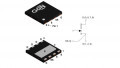
MasterGaN1. Image used courtesy of STMicroelectronics
ST’s newest product, dubbed MasterGaN, is a half-bridge 600 V gate driver IC based on silicon with a pair of GaN transistors on the same chip. The MasterGaN1 contains two enhancement mode transistors, a 10 A maximum current rating, and a 150 mΩ on-resistance (RDS(ON)).

Block diagram of the MasterGan1. Image used courtesy of STMicroelectronics
The logic inputs are compatible with signals from 3.3 V to 15 V, and the system also offers low-side and high-side UVLO protection, interlocking, a dedicated shutdown pin, and over-temperature protection.
A Simplified Option for Designers
Integrating these components onto the same IC is likely to result in simpler designs, a smaller footprint, easier assembly, and increased reliability (since there are fewer components).
ST expresses hope that its new product will “make a difference for smartphone ultra-fast chargers and wireless chargers, USB-PD compact adapters for PCs and gaming, as well as in industrial applications like solar-energy storage systems, uninterruptible power supplies, or high-end OLED TVs and server cloud."


Is that IC suitable to driver and speed control of the PMDC 180VDC 6.5A continues current Motor? Plan to 220VAC convert to DC via full wave rectification and then feed to motor..