 Facebook
 Google
 GitHub
 Linkedin
New Research Suggests Processing-in-Memory Could Revolutionize Analog Computing
Processing-in-memory is no longer confined to the research realm. Even companies like Samsung and IBM are spearheading the movement toward in-memory computing.
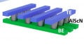
In a recent report, Chinese outlets have rumored that DAMO Academy—Alibaba's research center—has busted the von Neumann bottleneck with a breakthrough processing-in-memory (PIM) chip that stacks memory and logic in 3D. This isn't the first time a large company has turned to a vertical structure to shorten the distance between memory and computing. Several years ago, IBM published research on how 3D-stacked memory and byte-addressable resistive nonvolatile memory (NVM) introduce new ways for EEs to address PIM.

3D-stacked DRAM architecture. Image used courtesy of IBM
While Alibaba has yet to confirm these reports, this topic underscores how research in PIM is heating up, both at universities and among major semiconductor suppliers.
How PIM Rethinks a von Neumann Architecture
A conventional von Neumann computer architecture uses one subsystem for data storage and another for computation. Data and logic are separate.
To perform operations, data must be moved from DRAM storage to the CPU by sending a memory request to the memory controller, communicated through a narrow memory channel. But this movement from DRAM to CPU can create major bottleneck issues for the system—hiking up energy consumption while slowing down the exchange of multiple memory requests at once. This is how systems have always worked, at least since the widespread adoption of the digital binary model.

The von Neumann architecture. Image used courtesy of Srivats Shankar
A processing-in-memory (PIM) model rethinks the von Neumann architecture by merging computation and data—which is why PIM is also referred to as near-data processing.
Several research groups and corporations are creating PIM architectures to bring processing-in-memory closer to reality. Last year, All About Circuits discussed how many companies are finding that in-memory computing can solve the AI memory balancing act in terms of speed, volume, and processing.
This is because, unlike digital chips, PIM AI chips perform in the analog domain—something that Imec and Globalfoundries have dubbed "analog-in-memory computing (AiMC)" in a recent AI chip.
PIM Research Brings Analog Computing a Step Away from Digital
Now, a research team from Washington University in St. Louis led by Xuan "Silvia" Zhang has used resistors instead of transistors to build a PIM circuit that bypasses the limitations of the von Neumann architecture. Both the memory and the processor are in the resistor. Such placement of components makes translation from analog to digital or binary (1–0) unnecessary and simplifies the complex additions and multiplications necessary for AI calculations.
Instead of using transistors to open and close the gates and control the current to either flow or not flow—creating a sequence of 1s and 0s—the PIM circuit performs additions by connecting two currents and multiplications by tweaking the value of the resistor.

Working principle behind in-memory computing. Image used courtesy of Hazelcast
At some point, though, analog data must be converted into digital to be incorporated into today’s digital technologies. The researchers initially assumed this only entailed moving ADC (analog-digital conversion) one step further down the conversion hierarchy.
However, the team instead found that introducing a neural approximator increased the processing efficiency of individually-converted resistor columns in multiple directions: down, across, or in any other maximum-efficiency direction.
The most significant discovery made by Zhang’s team was that partial sums created by RRAM crossbar columns could be converted to digital format with a single ADC, no matter their number—18, 64, or 128—reducing the number of conversions at the outer edge as far as possible.
Samsung Backs Processing-in-Memory
The findings from Washington University broach an interesting question: Will analog drive the future of computing? Samsung’s recent investments into in-memory processing applications may answer that question.
Samsung is attempting to bridge the gap between memory and logic by integrating high-bandwidth memory (HBM) and processing-in-memory with an accelerator system. The result is an HBM-PIM architecture suitable for mobile and other commercial DRAM modules, including data centers and supercomputers.

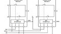
AXDIMM buffer chip with an in-built AI engine. Image used courtesy of Samsung
The acceleration in the DIMM (AXDIMM) buffer chip—a kind of multi-core processor that can process multiple memory ranks—is achieved with a built-in AI engine called a programmable computing unit (PCU). This device is said to increase the system’s performance by 2.5 times and reduce energy consumption by 60%.
Samsung has seen promising results for this PCU in image classification, speech recognition, and translation. SAP HANA is also collaborating with Samsung to improve an in-memory database management system (IMDBMS).
Will PIM Help Lift the Burden of Edge AI Processing?
As more processing demands are heaped on embedded systems, especially at the edge, manufacturers are looking for ways to cut down on the travel time to fetch data from memory. As PIM gains more traction in academic and industry spaces, in-memory computing may be a viable solution—especially as it is promoted by big names like Samsung and IBM.
Still, programmers face the challenging task of defining ways to communicate with the programming model. These engineers and system architects must also find solutions for data allocation issues and PIM runtime scheduling.


I think that if redundant slightly altered maps of analog state could be formed in PIM, efficiency would be increased when a different set queries of the same data occurs. Might make it easier for an AI to pass a Turing test or become sentient. The application of such could also move us a step closer to AI consciousness