Facebook
 Google
 GitHub
 Linkedin
Researchers Devise More Washable, Flexible, and Connected Electronics
Researchers are rethinking how electronics interact with the world, from fabrics that respond to gestures without touch to chips that generate terahertz waves without bulky components.
In this roundup, we take a look at three examples of recent research efforts to make electronics more durable and efficient. This includes washable, touchless e-textiles enabling intuitive human-computer interaction, chip-based terahertz wave generators for wireless data transmission, and 2D ferroelectrics unlocking new possibilities in ultra-thin memory and neuromorphic computing. These developments aren’t just improving technology—they’re changing how it fits into daily life.
Washable, Touchless E-Textiles for Wearables
Researchers from Nottingham Trent University, Helmholtz-Zentrum Dresden-Rossendorf, and the Free University of Bozen-Bolzano have developed a washable, touchless electronic textile that integrates flexible magnetoresistive sensors within braided yarns. This innovation overcomes longstanding issues with capacitive sensors, which are prone to accidental activation, by enabling touchless control through magnetic field detection.
Users can interact with the textile using a ring or glove embedded with a small magnet, making the fabric function as an intuitive human-computer interface. Unlike earlier e-textile prototypes relying on rigid PCBs, this approach embeds sensors directly into fibers, preserving the fabric's flexibility and washability.

The textile can be operated using a ring or glove. Image used courtesy of Free University of Bozen-Bolzano
The prototype features sub-millimeter-scale sensors seamlessly woven into textiles, enabling applications such as gesture-controlled clothing, VR navigation armbands, and self-monitoring safety straps. Its architecture ensures a rapid response time (<50 ms) and durability across diverse environments, including underwater use.
Potential applications span wearable health monitoring, interactive fashion, sports performance tracking, and industrial safety. Future research aims to enhance sensor sensitivity, miniaturize components for integration into finer fabrics, and develop energy-autonomous designs using printed micro-supercapacitors. With industrial-scale production in sight, this breakthrough sets the stage for smart textiles to become a seamless extension of daily life.
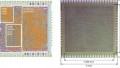
Scalable Chip-Based Terahertz Wave Generation
MIT researchers have developed a chip-based terahertz (THz) wave generator that eliminates the need for bulky silicon lenses while achieving record-high power output. By addressing the longstanding challenge of dielectric mismatch at the silicon-air boundary, the team introduced a thin, laser-patterned dielectric sheet affixed to the chip’s rear, significantly enhancing wave transmission efficiency.
This technique, inspired by microwave matching principles, minimizes reflection losses and enables >80% radiation efficiency. Coupled with Intel’s high-frequency FinFET transistors, the chip delivers a peak radiation power of 11.1 dBm—surpassing traditional CMOS-based THz sources.
_wave_generator.jpg)
The use of terahertz waves, which have shorter wavelengths and higher frequencies than radio waves, could enable faster data transmission, more precise medical imaging, and higher-resolution radar. Image used courtesy of MIT
The compact design facilitates scalable, high-density phased arrays with applications in security scanning, medical imaging, environmental monitoring, and next-generation 6G communications. Its high-frequency precision allows for non-ionizing sub-millimeter imaging, chemical detection, and ultra-fast wireless data transfer.
Future research aims to fabricate a 512-element phased array for dynamic beam steering, integrate III-V semiconductors for higher power output, and optimize on-chip power management. MIT’s collaboration with Intel’s University Shuttle Program is driving foundry-level scalability, paving the way for THz technology’s widespread adoption in electronics, sensing, and telecommunications.
Scalable 2D Ferroelectrics
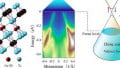
Researchers at the Hong Kong Polytechnic University (PolyU) have achieved a breakthrough in two-dimensional (2D) ferroelectric materials by developing phase-controllable indium selenide (In₂Se₃) films. By refining chemical vapor deposition (CVD) techniques and leveraging strain-induced phase transitions, the team has overcome previous limitations in large-scale synthesis and phase stability. This work advances the field by controlling the production of centimeter-scale, high-purity α-phase films, which exhibit superior electrical performance for memory, microelectronics, and AI applications.
The PolyU research team has revealed the mechanisms for the synthesis and applications of materials through atomic resolution. Image used courtesy of PolyU
The new In₂Se₃-based ferroelectric field-effect transistors demonstrate high carrier mobility (53 cm²/Vs) and robust non-volatile memory characteristics, surpassing conventional 2D materials like MoS₂. The research also explores twisted bilayer In₂Se₃, revealing tunable polar vortices that could lead to novel quantum computing architectures. Future work includes transitioning from CVD to industrial-scale metal-organic CVD (MOCVD) for wafer-scale production, integrating In₂Se₃ with silicon-based CMOS for FeRAM, and leveraging strain engineering for next-generation neuromorphic computing.