 Facebook
 Google
 GitHub
 Linkedin
DMA Digital-to-Analog Conversion with a SAM4S Microcontroller: The Timer/Counter
Part One in this three-article series focuses on using the SAM4S timer/counter peripheral to precisely control the DAC’s sampling rate.
Part One in this three-article series focuses on using the SAM4S timer/counter peripheral to precisely control the DAC’s sampling rate.
Supporting Information
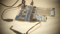
- Intro to Project Development with the Atmel SAM4S Xplained Pro
- Introduction to Digital–Analog Conversion
Required Hardware/Software
A Real DAC
If you read my recent article in which I analyze the performance of a pulse-width-modulation-based digital-to-analog converter, you know that PWM DACs are far from impressive. However, the PWM DAC lives on, in part because (as mentioned in another article on the same topic) many microcontrollers do not incorporate dedicated DAC hardware. This relatively common “lack of DAC”—along with my general reluctance to complicate a design with external components that would be thoroughly unnecessary if IC manufacturers would be so kind as to make microcontrollers exactly the way I want them—explains my great satisfaction when I find myself using a microcontroller that does indeed have a real DAC. This satisfaction reaches new heights with the SAM4S series devices, which provide not one but two digitally controlled analog outputs.
The goal of this project is to generate a sine wave using the SAM4S DAC module. This task alone is sufficiently nontrivial thanks to the somewhat labyrinthine relationship between the SAM4S datasheet, the Atmel Software Framework (ASF), the ASF documentation, and the microcontroller’s actual hardware. This nontriviality notwithstanding, we will go a step further by feeding data to the DAC via direct memory access (DMA) instead of CPU instructions. We’ll talk more about DMA in Part 3.
Though I enjoy looking at sine waves on my oscilloscope, this project is not really an end in itself. Rather, it is 1) a vehicle for exploring important SAM4S capabilities, namely precision timing/counting, DMA, and integrated digital-to-analog conversion; and 2) a foundation for other projects that require synchronous, CPU-efficient digital-to-analog conversion, such as synthesizing audio signals or generating baseband waveforms for a software-defined radio.
Free-Running vs. Triggered
It is possible to use the DAC by simply writing a value to the DAC’s conversion-data register. This is referred to as free-running mode. The analog output voltage is updated as soon as you write the data (actually, 25 DAC clock ticks after you write the data—more on DAC hardware details in Part 2). This is fine for some applications, but for accurate synthesis of periodic signals (such as a sinusoid), we need to ensure that all the output-voltage updates are separated by identical intervals. To this end, we will use triggered mode, in which a write to the conversion-data register does not actually modify the output voltage until the DAC hardware is triggered by a separate timing signal. The SAM4S datasheet (page 1124) refers to this trigger as “external,” which is somewhat misleading—in my experience “external” usually means “external to the chip,” whereas in this case it means “external to the DAC module.” Here are the trigger-signal options:

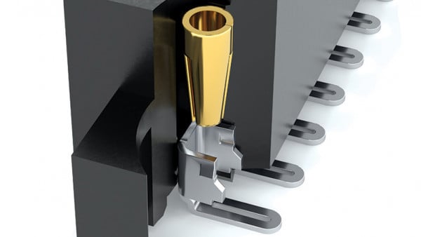
We will be using the TIO signal from timer/counter channel 1, because we can conveniently probe this signal via terminal 1 in the row of through-holes labeled “PIOD INTERFACE”:

As indicated in the photo, this terminal 1 is connected to pin A15, and the SAM4S datasheet (page 52) tells us that we can drive signal TIOA1 on PA15 by connecting this pin to peripheral B:

The “A” after TIO indicates that this is the first of two output signals (TIOA and TIOB) that each timer/counter channel can generate; the “1” after “TIOA” refers to channel 1 of the timer/counter module, which includes three identical, independent channels.
Waveform vs. Capture
A timer/counter channel can be configured for waveform mode or capture mode. In capture mode, TIOA and TIOB are inputs; a signal connected to TIOA or TIOB can be used to tell the timer/counter hardware to store the current counter value in a separate register. This functionality is useful for measuring pulse width or the delay between two pulses. We, however, want to generate a timing signal, not measure one, so we need waveform mode. This name reflects the timer/counter’s ability to generate a variety of digital waveforms by means of the three compare registers and different counting modes. Our task is pretty straightforward though—we just need a square wave with frequency equal to our desired DAC sample rate. Thus, we can use the up-counting-only mode, and we need only one compare register.
The first thing to do is choose the clock that will drive the counter register. Here are the options:

We will configure the microcontroller for a master clock (MCK) frequency of 96 MHz; the reason for this will be explained in Part 2. The desired DAC sample rate is 1 MHz, and MCK/8 (i.e., 12 MHz) is a good choice for generating a 1 MHz DAC trigger because the required divider value is an integer.
Now that we know the frequency of the clock source for the counter, we need to choose the proper value for “Register C,” abbreviated RC. This rather cryptically named register can be used to reset the counter when it reaches the value held in RC, as follows:

So, if we set the WAVESEL bits in the “TC Channel Mode” register to binary 10 and then load the proper compare value into RC, we will have a counter that resets and starts counting up from 0 when the counter value equals RC. The only thing left is to tell the timer/counter channel to modify the logic level of TIOA every time this match occurs. We do this by means of the ACPC field in the channel mode register:

We will use the toggle option. The following diagram conveys the relationship between the RC compare value and the waveform generated on TIOA.

Firmware
Now it’s time to translate all this timer/counter business into code, and for this we turn (as usual) to the ASF. First, let’s add all the ASF modules we will need for the entire project:

The modules underlined in green are the ones you need to add (the others are included automatically by Atmel Studio).
Next we have two preprocessor definitions:
//Port I/O
#define TC0_TIOA_CH1 IOPORT_CREATE_PIN(PIOA, 15)

//Timer configuration
#define TC0_CHANNEL1 1
The first attaches a name to pin A15, and the second allows us to refer to timer/counter channel 1 with TC0_CHANNEL1 instead of the rather less informative numeral 1.
Next we need to enable the peripheral clock for the timer/counter. There is a detail here that I consider quite confusing, so take note of the following discussion—it might help you avoid a good bit of frustration some day. The confusion relates to the question of which peripheral ID to use with the pmc_enable_periph_clk() function. In my opinion, the obvious answer is ID_TC0, because we are working with channel 1 in timer/counter module 0. This reality is reflected in the timer/counter channel-initialization function, tc_init()—the first argument is TC0 or TC1 (referring to timer/counter module 0 or module 1) and the second argument is the channel number. It seems only natural that the peripheral ID should correspond to the peripheral module itself, not to one of the channels within the module. But as you have probably guessed by now, such is not the case. As it turns out, the peripheral clock is enabled or disabled for individual timer channels. To compound the confusion, the SAM4S datasheet (page 50) refers to these channels as follows:

So with the peripheral identifiers, we have timer/counter channel 0 through 5, whereas elsewhere we have timer/counter module 0 channel 0 through 2 and timer/counter module 1 channel 0 through 2. So anyways, just be aware that you have to enable the peripheral clock for each timer/counter channel that you are using, with peripheral ID channels 0–2 corresponding to module 0 channels 0–2, and peripheral ID channels 3–5 corresponding to module 1 channels 0–2.
After enabling the peripheral clock via pmc_enable_periph_clk(ID_TC1), we configure the timer/counter channel:
tc_init(TC0, TC0_CHANNEL1,
        TC_CMR_TCCLKS_TIMER_CLOCK2    //MCK/8
    |     TC_CMR_WAVE    //waveform mode
    |    TC_CMR_WAVSEL_UP_RC    //count up, reset on RC match
    |    TC_CMR_ACPC_TOGGLE    //toggle TIOA on RC match
    );
With the tc_init() function, you first specify the timer/counter module and the channel within the module, then you use the logical OR operator along with ASF preprocessor definitions (found in “tc.h”) to specify the proper values for whichever fields need to be modified in the channel mode register. As indicated by the comments in the above code excerpt, we are configuring the channel for
- MCK/8 clock source,
- waveform mode,
- up-counting-only mode with automatic reset when the counter value equals RC, and
- TIOA toggle when the counter value equals RC.
From the above diagram, we know that the value in RC should be 6 to produce a 1 MHz clock:
\[f_{TIOA}=\frac{12\ MHz}{2\times RC}\ \ \Rightarrow\ \ RC=\frac{12\ MHz}{2\times1\ MHz}=6\]
tc_write_rc(TC0, TC0_CHANNEL1, 6);
Now all we need to do is enable the timer/counter channel with a call to tc_start():
tc_start(TC0, TC0_CHANNEL1);
Results and Conclusion
You can use the following link to download the source and project files for this stage of the project:
Here is a scope capture of the resulting waveform:

Now that we have our sample-rate signal just the way we want it, we are ready to fire up the DAC. In the next article we will explore the SAM4S DAC controller (DACC) peripheral, the electrical characteristics of the DAC itself, and the ASF’s DACC module.
Next Article in Series: Understanding and Using the SAM4S Digital-to-Analog Converter
Give this project a try for yourself! Get the BOM.


Is the mapping of the TIOA counter reload,
pmc_enable_periph_clk(ID_TC1);
pio_configure_pin(TC0_TIOA_CH1, PIO_TYPE_PIO_PERIPH_B);
only as a debug test-point? i.e. does the dac need this pio mapping in order to have it pause in between dma transfers?