Facebook
 Google
 GitHub
 Linkedin
The PGA2311 Stereo Audio Volume Control: A High-Performance Digital Volume Board
Featuring 0.0004% THD+N and a 120 dB dynamic range, this design drives 600 Ω loads directly via a 3-wire serial interface. Zero-crossing detection ensures click-free level steps.
The Stereo Audio Volume Control is a compact board built around the Texas Instruments PGA2311, a precision digital volume control IC with an integrated, high-performance operational amplifier. The device delivers very low noise and distortion, making it suitable for professional and high-end consumer audio systems. The board breaks the PGA2311 out to pin headers and four 3.5 mm stereo sockets (Figure 1).
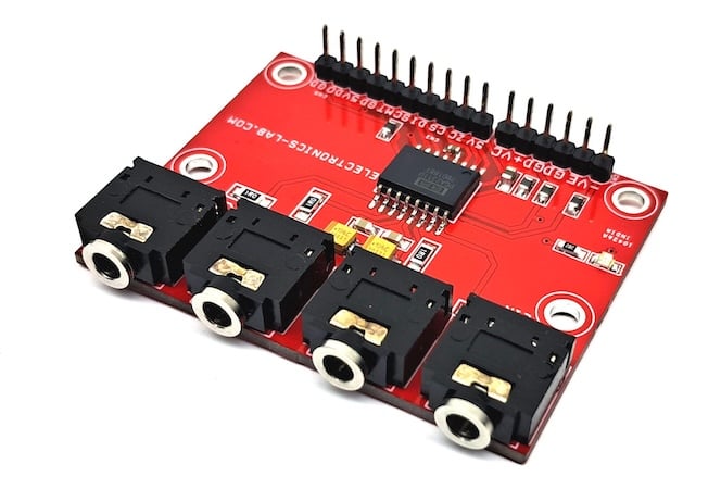
Figure 1. The assembled Stereo Audio Volume Control board.
The PGA2311 can drive loads as low as 600 Ω directly, with no additional buffering. A host controller sets the volume over a 3-wire serial interface, so the module connects easily to a wide range of microcontrollers. Multiple PGA2311 devices can also be daisy-chained for multi-channel applications.
The board runs from a dual ±5 V analog supply and a +5 V digital supply. Ferrite beads and decoupling capacitors filter the supply rails.
Specs and Features
- Analog power supply: ±5 V DC (dual supply)
- Digital power supply: +5 V DC
- Two independent audio channels (left and right)
- 3-wire serial control interface
- Gain range: +31.5 dB to –95.5 dB in 0.5 dB steps
- Dynamic range: 120 dB, with 0.0004% THD+N at 1 kHz
- Zero-crossing detection for click-free, noise-free level changes
- Hardware and software mute
- Low inter-channel crosstalk
- Drives loads as low as 600 Ω
- PCB dimensions: 55.39 × 42.66 mm
- Four 3 mm PCB mounting holes
How It Works
The PGA2311 has two independent channels, left and right. As the block diagram in Figure 2 shows, a serial control port loads an 8-bit gain value for each channel and sets the gain of that channel's amplifier stage.
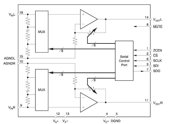
Figure 2. Block diagram of the PGA2311. Image used courtesy of Texas Instruments.
Analog Inputs and Outputs
Each channel has its own input and output pin. The inputs are VINL (pin 16) and VINR (pin 9), and the outputs are VOUTL (pin 14) and VOUTR (pin 11). All signals are unbalanced and referenced to analog ground (AGNDL and AGNDR).
The input and output swing must stay within 1.25 V of the analog supply rails. With ±5 V supplies, the maximum signal swing is approximately 7.5 V peak-to-peak. A low source impedance gives the best performance. A source impedance of 600 Ω or less is ideal, and up to 2 kΩ causes minimal THD+N degradation.
Gain Settings
An 8-bit register sets the gain of each channel: L[7:0] for the left channel and R[7:0] for the right. A value of N = 0 mutes the channel by connecting its input to analog ground. For N = 1 to 255, the gain is:
Gain (dB) = 31.5 – [0.5 × (255 – N)]
The gain changes in precise 0.5 dB steps.
Zero-Crossing Detection and Mute
The zero-crossing feature gives smooth, click-free volume changes. It is enabled when ZCEN (pin 1) is high and disabled when ZCEN is low. When enabled, a gain change takes effect only when the input signal crosses zero or after a 16 ms timeout. This minimizes audible clicks and pops.
Muting works in two ways:
- Hardware mute: Pulling the MUTE pin low disconnects the output buffers, and the outputs are internally terminated with 10 kΩ resistors to ground. The mute engages at a zero crossing or after a 16 ms timeout. It also performs an internal offset calibration.
- Software mute: Loading all zeroes into the gain register sets the internal amplifier to unity gain and connects the input to analog ground.
Serial Interface and Daisy-Chaining
The PGA2311 uses a simple 3-wire serial interface, plus a serial data output for chaining devices:
- CS (pin 2): Chip select, active low.
- SDI (pin 3): Serial data input, which receives the 16-bit control word.
- SCLK (pin 6): Serial clock. Data is latched on the rising edge.
- SDO (pin 7): Serial data output, used for daisy-chaining. It is tri-state and goes high-impedance when CS is high.
The 16-bit control word holds 8 bits of gain data for the left channel and 8 bits for the right channel. The data is sent MSB first in straight binary coding. Figure 3 shows the typical connection between a host controller and the PGA2311.
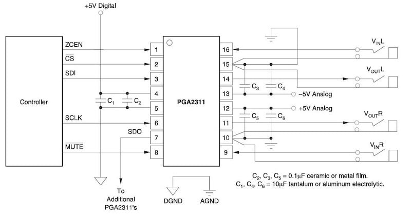
Figure 3. Typical connection diagram for the PGA2311 and a host controller. Image used courtesy of Texas Instruments.
Multiple devices can share the same CS and SCLK lines and be controlled through one SDI line. As Figure 4 shows, the SDO pin of each device feeds the SDI pin of the next. This reduces the number of control lines needed and suits multi-channel audio systems.
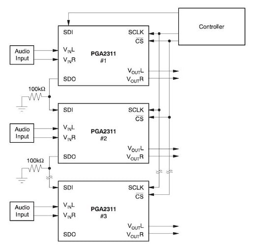
Figure 4. Daisy-chaining multiple PGA2311 devices. Image used courtesy of Texas Instruments.
Schematic and Bill of Materials
The schematic is shown in Figure 5. Each audio input and output passes through a 1 Ω series resistor (R2 to R5). Optional 2-pin headers (CN3, CN4, CN6, and CN7) provide an alternative to the stereo sockets.
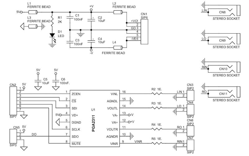
Figure 5. Schematic of the Stereo Audio Volume Control board.
The bill of materials is shown in Table 1.
Table 1. BOM for Stereo Audio Volume Control PGA2311.
| REF | DESCRIPTION | QTY | MFG | SUPPLIER | PART NO. |
| CN1 | 6-pin male header, 2.54 mm pitch | 1 | WURTH | DigiKey | 732-5319-ND |
| CN2 | 7-pin male header, 2.54 mm pitch | 1 | WURTH | DigiKey | 732-5320-ND |
| CN3, CN4, CN6, CN7 | Optional (DNP) | 4 |
|
DigiKey |
|
| CN5 | 3-pin male header, 2.54 mm pitch | 1 | WURTH | DigiKey | 732-5316-ND |
| C1, C3 | 100 nF/50 V ceramic, SMD 0805 | 2 | YAGEO/MURATA | DigiKey |
|
| C2, C4 | 10 µF/16 V tantalum, SMD 1210 | 2 | KEMET | DigiKey |
|
| C6 | 100 nF/50 V ceramic, SMD 0805 | 1 | YAGEO/MURATA | DigiKey |
|
| D1 | LED, red, SMD 0805 | 1 | OSRAM | DigiKey | 475-1278-1-ND |
| L1, L2, L3, L4 | Ferrite bead, 600 Ω | 4 | LAIRD | DigiKey | 240-2394-1-ND |
| R1 | 2 kΩ, 5%, SMD 0805 | 1 | YAGEO/MURATA | DigiKey |
|
| R2, R3, R4, R5 | 1 Ω, 5%, SMD 1206 | 4 | YAGEO/MURATA | DigiKey |
|
| U1 | PGA2311 | 1 | TI | DigiKey | 296-48643-1-ND |
| CN8, CN9, CN10, CN11 | 3.5 mm stereo female socket | 4 | CUI AUDIO | DigiKey | CP1-3525N-ND |
| C5 | 10 µF/25 V ceramic, SMD 0805 | 1 | YAGEO/MURATA | DigiKey |
|
Connections
The connection diagram in Figure 6 shows the function of each header pin and socket.
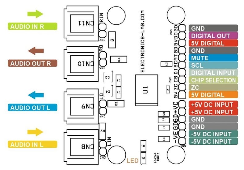
Figure 6. Connection diagram for the Stereo Audio Volume Control board.
CN1 — Power Header (6-pin, 2.54 mm pitch):
- Pins 1 and 2 = +VCC (+5 V DC)
- Pins 3 and 4 = GND
- Pins 5 and 6 = –VEE (–5 V DC)
CN2 — Control Header (7-pin, 2.54 mm pitch):
- Pin 1 = 5 V DC (digital)
- Pin 2 = ZCEN
- Pin 3 = Chip Select (CS)
- Pin 4 = SDI
- Pin 5 = SCLK
- Pin 6 = MUTE
- Pin 7 = GND
CN5 — Digital Output Header (3-pin, 2.54 mm pitch):
- Pin 1 = 5 V DC (digital)
- Pin 2 = Digital Output (SDO)
- Pin 3 = GND
Audio Connectors:
- CN3, CN4, CN6, CN7 = Optional audio input and output headers
- CN8 = 3.5 mm stereo female socket, left audio input
- CN9 = 3.5 mm stereo female socket, left audio output
- CN10 = 3.5 mm stereo female socket, right audio input
- CN11 = 3.5 mm stereo female socket, right audio output
Indicator:
- D1 = Analog power LED
PCB Files
The board measures 55.39 × 42.66 mm and has four 3 mm mounting holes. Figures 7 and 8 show the top and bottom PCB layouts.
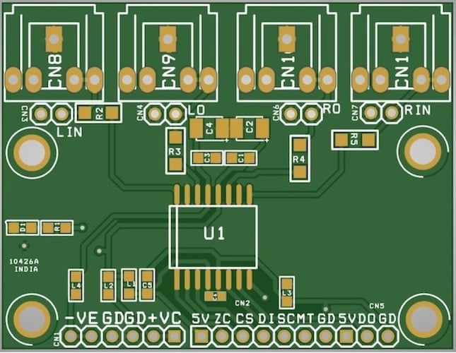
Figure 7. PCB layout, top layer.
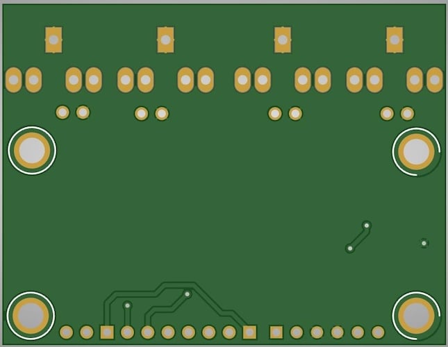
Figure 8. PCB layout, bottom layer.
You can download the layout files for this project here:
Stereo Audio Volume Control Gerber Files
Except where noted, all images used courtesy of Rajkumar Sharma
Related Content