Facebook
 Google
 GitHub
 Linkedin
The Actively Loaded MOSFET Differential Pair: Measuring Lambda, Predicting Gain
In this article, we’ll look at the equation for differential gain and use LTspice to find the value of the channel-length-modulation parameter referred to as lambda (λ).
In this article, we’ll look at the equation for differential gain and use LTspice to find the value of the channel-length-modulation parameter referred to as lambda (λ).
Supporting Information
- Discrete Semiconductor Circuits: Differential Amplifier
- Discrete Semiconductor Circuits: Simple Op-Amp
- Insulated-Gate Field-Effect Transistors (MOSFET)
- The Basic MOSFET Constant-Current Source
- The Basic MOSFET Differential Pair
- SPICE models for 0.35 µm MOSFETs
Previous Articles
- The MOSFET Differential Pair with Active Load
- Advantages of the Actively Loaded MOSFET Differential Pair
- The Actively Loaded MOSFET Differential Pair: Output Resistance
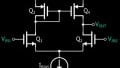
The Diff Pair with Output Resistance
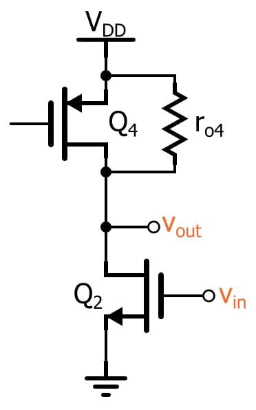
In the previous article, we discussed MOSFET small-signal output resistance (ro): why it exists, how it affects an amplifier circuit, and how to calculate it. Now we will use this newfound expertise to examine the gain of the actively loaded differential pair. Let’s start with the following circuit:
So now we have drain resistors for our amplifier FETs, which makes the actively loaded configuration resemble the drain-resistor version presented in The Basic MOSFET Differential Pair. A full differential-gain analysis for this circuit is not exactly simple, and I don’t want to get bogged down in the complexity of it all. Instead, we’ll take a conceptual, intuitive approach.
The easiest way to proceed is to assume that the circuit is symmetrical and then analyze only the right-hand side of the diff pair (because the output is taken from the right-hand side). This technique would be fine with the drain-resistor diff pair because that circuit is actually symmetrical if we assume perfect matching. But the actively loaded diff pair, unfortunately, is not symmetrical.
However, it turns out that we can pretend that the circuit is symmetrical and then perform an intuitive analysis on the right-hand side of the pair. In so doing, we can arrive at a correct expression for differential gain. (I say “a correct expression” instead of “the correct expression” because even the more formal analysis that leads to this expression involves simplifications.)
Maybe you don’t like this sort of reckless disregard for rigorous circuit theory, but I’m just glad that I can examine and (at least partially) understand the situation without getting lost in the details.
The “Intuitive” Analysis
So, let’s split the circuit in half and assume a virtual ground connected to the source of Q2.
We can see that the circuit resembles the right-hand side of the drain-resistor version. As stated in The Basic MOSFET Differential Pair, the magnitude of the differential gain of the full drain-resistor diff pair is (gm × RD), and this means that the gain of one side of the drain-resistor diff pair (AV,OS) is this same expression divided by two:
$$A_{V,OS}=\frac{g_m\times R_D}{2}$$
We can apply this same expression to the actively loaded pair, where the drain resistor is now the small-signal output resistance of Q4. Don’t forget, though, that the diff pair converts the output from differential to single-ended without loss of gain—in other words, the factor-of-two reduction that occurs when we split the drain-resistor diff pair does not apply to the active-load configuration.
Thus, we might conclude that the gain of the actively loaded differential pair (AV,AL) is the following:
$$A_{V,AL}=g_m\times r_{o4}$$
But this would be wrong! It’s wrong because we are forgetting about the output resistance of Q2. With the drain-resistor diff pair, it is more justifiable to ignore the output resistance of Q2 because it is probably much larger than the drain resistor. As we saw with the common-source amplifier discussed in the previous article, small-signal analysis places the output resistance in parallel with the drain resistor.
If ro is much larger than RD, the parallel combination won’t be much different from RD. But we have a whole new situation with the actively loaded circuit: ro of Q4 is likely to be quite similar to ro of Q2, and thus we cannot ignore ro of Q2.
So we need a new circuit diagram:
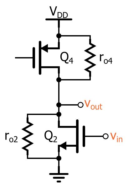
Now the overall output resistance is ro2||ro4, and we rightly conclude that the gain of the actively loaded differential pair is the following:
$$A_{V,AL}=g_m\times \left(r_{o4}\parallel r_{o2}\right)$$
where gm refers to the transconductance of the amplifying transistors (Q1 and Q2), not that of the current-mirror transistors (Q3 and Q4).
Measuring Lambda
At this point, we want to predict the gain of our actively loaded diff pair—but we can’t, because we need to know the value of ro4 and ro2.
For this we need to know lambda, because
$$r_o=\frac{1}{\lambda\times I_D}$$
I know what you’re thinking: Just look in the SPICE model!
Alas, it’s not always that simple. The MOSFET models we’re using in our simulations are of the “BSIM3” variety, which means they are too sophisticated for the lambda-based approach to channel-length modulation. In other words, you won’t find lambda in the SPICE model because it has been replaced by other parameters that allow for a more accurate simulation.
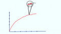
So, we have here a good opportunity to determine lambda empirically. How do we go about that? Well, consider the following graph of drain current vs. drain-to-source voltage:
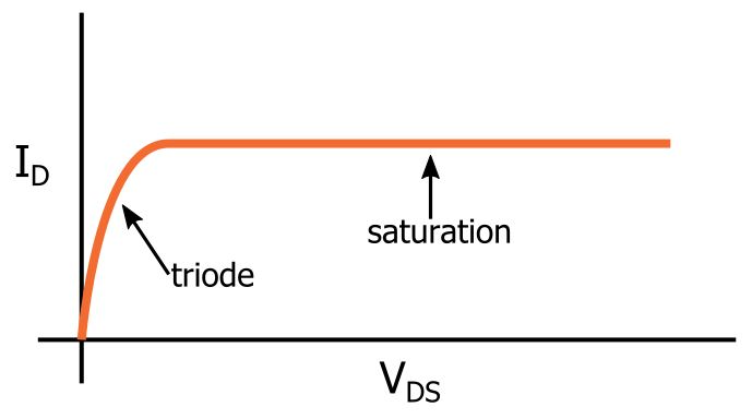
First, we apply a gate-to-source voltage that is high enough to bring the FET out of cutoff. Then, holding VGS constant, we increase the drain-to-source voltage. As VDS becomes high enough to pinch off the channel, the FET enters saturation. If we ignore channel-length modulation, the curve will be perfectly flat (as shown above), because increases in VDS have no effect on drain current.
The following curve, in contrast, is not flat in the saturation region because it incorporates channel-length modulation:
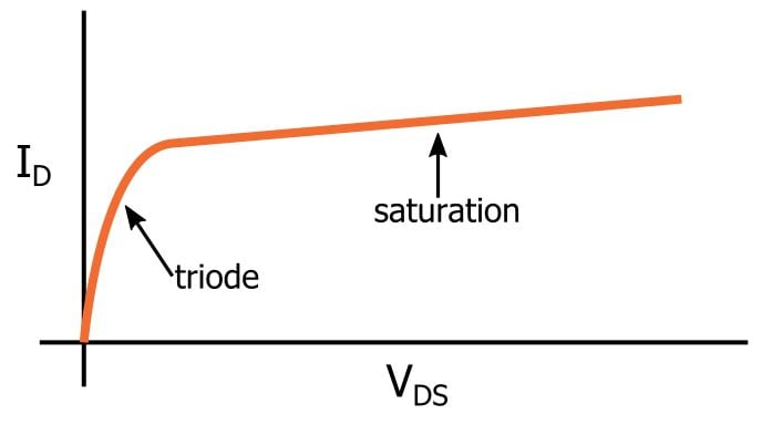
The gradual increase in saturation-region drain current corresponds to the additional current flowing through the output resistance as the drain-to-source voltage increases. If we extend this line back to the x-axis, we have lambda:
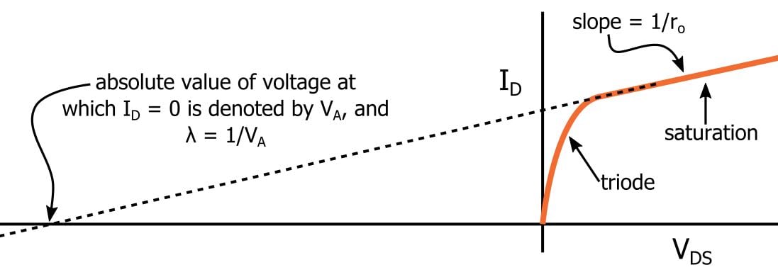
As indicated in the plot, you can also measure the slope and convert this directly to ro.
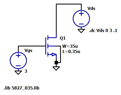
The Lambda Simulation
Here is the LTspice circuit that I used for finding lambda:
And here is the corresponding plot of drain current vs. drain-to-source voltage:
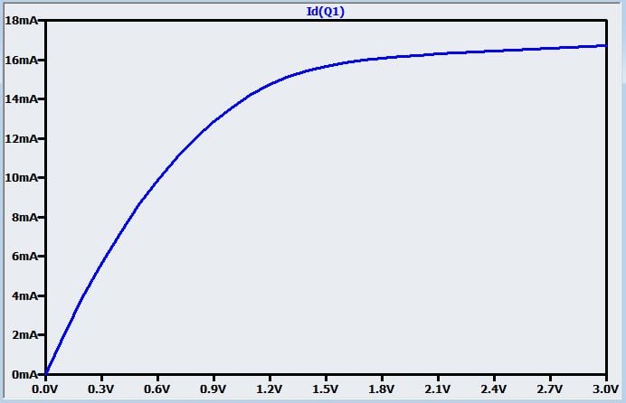
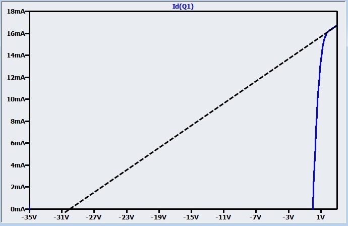
We’ll use a simple graphical method to obtain an approximate value for lambda:
The Gain Calculation
So let’s say that λ ≈ 1/(30 V) = 0.033 V–1. In the simulations performed for a previous article, we used IBIAS = 500 µA, which corresponds to a DC-bias drain current of 250 µA for Q2 and Q4.
Thus, we have
$$r_o=\frac{1}{\lambda\times I_D}=\frac{1}{0.033\ V^{-1}\times 250\ \mu A}\approx 121\ k\Omega$$
Just to save ourselves a little trouble, we’ll use this value for ro of both the NMOS and the PMOS, though in reality we cannot assume that λPMOS = λNMOS. From a previous article (refer to the calculations at the end of the “Differential Gain” section), we know that gm for our NMOS transistors is 0.00182 A/V. Thus, we calculate our gain as follows:
$$A_{V,AL}=g_m\times (r_{o4}\parallel r_{o2})=0.00182\ \frac{A}{V}\times(121\ k\Omega \parallel 121\ k\Omega)\approx110$$
I checked this number against a simulation, and the results were not even close. The simulated gain was around 22.
It’s discouraging when simulations don’t confirm calculations, but in this case it’s not too surprising. On the contrary, the discrepancy reminds us that our simplified models are far less accurate with short channel lengths (I used 0.35 µm in the simulation). In fact, one of the documents (PDF) that accompanies the FET SPICE models that we’re using states the following: “Beware: do not expect very accurate results using hand calculations, especially for short channel lengths (L < 2 μ).”
The good news is that I got much better results when I increased the simulation channel lengths to 2 µm (I also increased the channel widths to maintain the same W/L ratio). The document mentioned above suggests a lambda of 0.025 V–1 for NMOS and 0.019 V–1 for PMOS with L = 2 µm; this gives ro2 = 160 kΩ and ro4 ≈ 211 kΩ, and thus AV,AL ≈ 166. This is much more consistent with the simulated gain, which was approximately 176.
Conclusion
We’ve covered quite a bit in this series on the actively loaded MOSFET differential pair. I hope you now have a solid understanding of the advantages and fundamental input–output characteristics of this important circuit.
Related Content