Facebook
 Google
 GitHub
 Linkedin
Si Lab - Simple Op Amp
Project Overview
This circuit design improves on the previous differential amplifier circuit project. As illustrated in Figure 1, there are two primary advantages of this new circuit:
- A current mirror comprised of NPN transistors, Q5 and Q6, is used to improve the bias current stability to the differential pair, Q3 and Q4. This replaces a simple resistor.
- A second current mirror using PNP transistors, Q1 and Q2, replaces the load resistor. The high impedance of this current mirror increases the voltage gain of the amplifier.
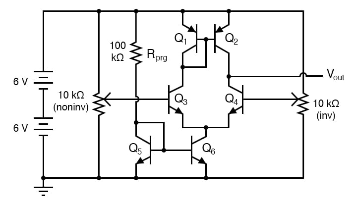
Figure 1. Schematic diagram of an op amp with differential inputs and current mirror load.
With a higher voltage gain, this circuit is able to function as a working operational amplifier or op amp. Op amps form the basis of a great many modern analog semiconductor circuits, so understanding the internal workings of an op amp is important. The PNP transistors, Q1 and Q2, form a current mirror that tries to keep the current split equally through the two differential pair transistors, Q3 and Q4. NPN transistors, Q5 and Q6, form another current mirror, setting the total differential pair current at a level predetermined by resistor Rprg.
Parts and Materials
- Two 6 V batteries
- Four NPN transistors—models 2N2222 or 2N3403 recommended
- Two PNP transistors—models 2N2907 or 2N3906 recommended
- Two 10 kΩ potentiometers, single-turn, linear taper
- One 270 kΩ resistor
- Three 100 kΩ resistors
- One 10 kΩ resistor
Learning Objectives
- Design of a differential amplifier circuit using current mirrors.
- Effects of negative feedback on a high-gain differential amplifier.
Instructions
Step 1: Build the op amp circuit shown in the circuit schematic of Figure 1 and the breadboard implementation of Figure 2.
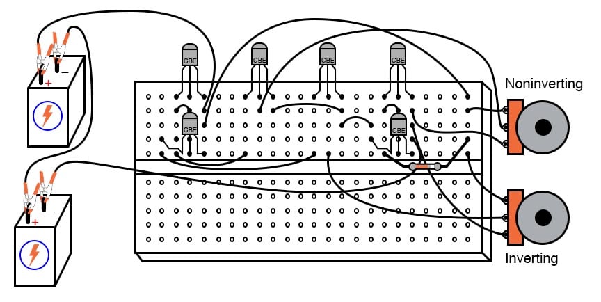
Figure 2. Breadboard implementation of an op amp with differential inputs and current mirror load.
Open-loop Op Amp Functioning as a Comparator
Step 2: Using the left potentiometer in Figure 1, set the input voltage to the base of the transistor, Q3, to 2.5 V.
Step 3: Using the other potentiometer, set the initial input voltage of the transistor, Q4, to 2.0 V. Measure the output voltage at the collector of Q4 with respect to the ground.
Step 4: Using the right potentiometer, slowly sweep the input voltage to the transistor, Q4, while monitoring the output voltage. The high voltage gain of this circuit means the circuit will function effectively as a comparator. The output voltage will rapidly change from high to low as the two input voltage signals approach and cross equality.
Step 5: Using the right potentiometer in Figure 1, set the input voltage to the base of the transistor, Q4, to 2.5 V.
Step 6: Using the left potentiometer, set the initial input voltage to the transistor, Q3, to 2.0 V. Again, measure the output voltage at the collector of Q4.
Step 7: Slowly sweep the input voltage to the transistor, Q3, while monitoring the output voltage. Notice how the input potentiometers have different effects on the output voltage. The input to the left transistor, Q3 (V+), drives the output voltage in the same direction (noninverting), while the input to the right transistor, Q4 (V-), drives the output voltage in the opposite direction (inverting). The op amp amplifies the difference between the two inputs.
Using the Op Amp as a Voltage Follower
Once the circuit’s differential response has been proven (the output voltage sharply transitions from one extreme level to another when one input is adjusted above and below the other input’s voltage level), you are ready to use this op amp in a circuit. The simple op amp circuit of Figure 3 is called a voltage follower and is a good configuration to try first.
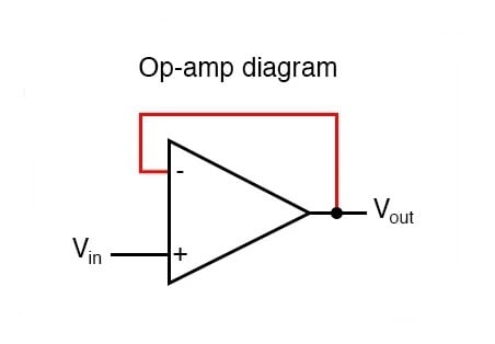
Figure 3. Op amp connected as a voltage follower using negative feedback.
Note in Figure 3 that the triangular op amp has its inverting and noninverting inputs designated with (-) and (+) symbols, respectively. The op amp output terminal is at the right of the symbol.
Step 8: To make a voltage follower circuit, directly connect the output of the amplifier to its inverting input. This means connecting the collector and base terminals of Q4 together, and removing the right, inverting potentiometer from the circuit, as illustrated in Figures 4 and 5.
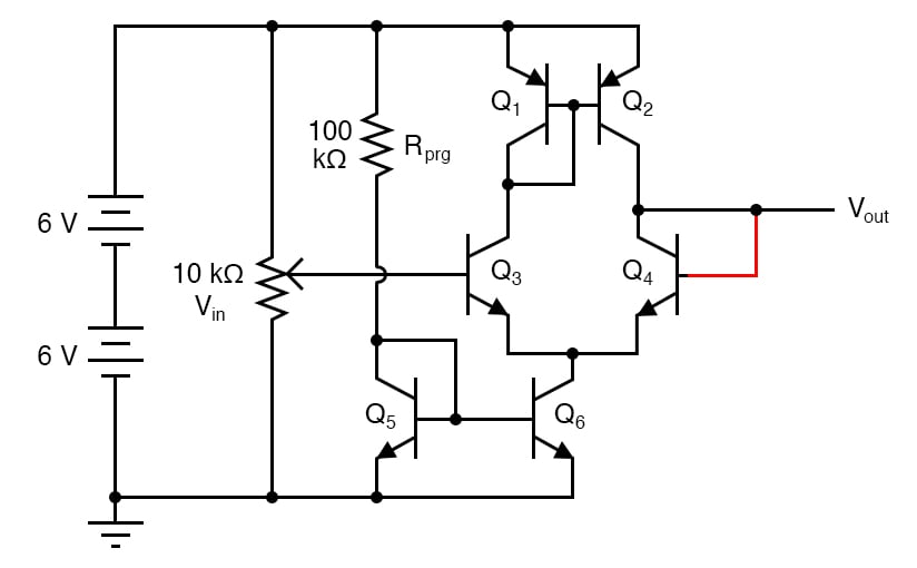
Figure 4. Schematic diagram of the op amp connected as a voltage follower.
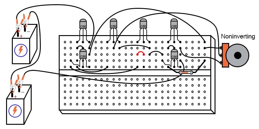
Figure 5. Breadboard implementation of the op amp connected as a voltage follower.
In both figures, the feedback wire connecting the output to inverting input is shown in red.
Step 9: As a voltage follower, the output voltage should follow the input voltage closely, deviating no more than a few hundredths of a volt. Measuring the input and output voltages to the op amp as you vary the potentiometer. This is a much more precise follower circuit than that of a single common-collector transistor, described in an earlier experiment!
Using the Op Amp in a Noninverting Amplifier Circuit
A more complex op amp circuit is called the noninverting amplifier, and it uses a pair of resistors in the feedback loop to feedback a fraction of the output voltage to the inverting input, causing the amplifier to output a voltage equal to some multiple of the voltage at the non-inverting input.

Figure 6. Op amp connected as a noninverting amplifier.
Step 10: Build the noninverting amplifier circuit illustrated in Figures 7 and 8.
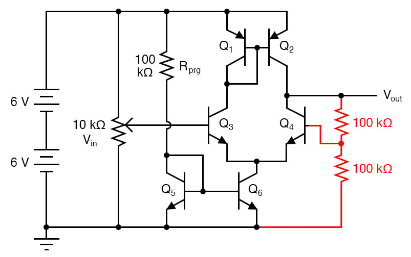
Figure 7. Schematic diagram of the op amp connected as a noninverting amplifier.
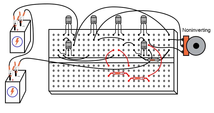
Figure 8. Breadboard implementation of the op amp connected as a noninverting amplifier.
If we use two equal-value resistors, the feedback voltage will be 1/2 the output voltage, causing the output voltage to become twice the voltage impressed at the noninverting input. Thus, we have a voltage amplifier with a precise gain of two.
Step 11: Measure the input and output voltages as you vary the potentiometer. As you test this noninverting amplifier circuit, you may notice slight discrepancies between the output and input voltages.
According to the feedback resistor values, the voltage gain should be exactly two. However, you may notice deviations in the order of several hundredths of a volt between what the output voltage is and what it should be. These deviations are due to imperfections in the differential amplifier circuit and may be greatly diminished if we add more amplification stages to increase the differential voltage gain.
Changing the Bias Current of the Differential Input Transistor Pair
Step 12: One way we can maximize the precision of the existing circuit is to change the resistance of Rprg. This resistor sets the lower current mirror’s control point and, in so doing, influences many performance parameters of the op amp. Try substituting difference resistance values, ranging from 10 kΩ to 1 MΩ. Do not use a resistance less than 10 kΩ, or else the current mirror transistors may begin to overheat and thermally run away.
Some operational amplifiers available in prepackaged units provide a way for the user to similarly program the differential pair’s current mirror and are called programmable op amps. Most op amps are not programmable and have their internal current mirror control points fixed by internal resistance, trimmed to precise value at the factory.
Related Content
Learn more about the fundamentals behind this project in the resources below.
Textbook:
Worksheets:
- Bipolar Transistor Biasing Circuits Worksheet
- Bipolar Junction Transistor (BJT) Theory Worksheet
- Differential Transistor Amplifiers Worksheet