 Facebook
 Google
 GitHub
 Linkedin
Si Lab - Multi-stage Amplifier
Project Overview
In this project, three BJT common-emitter amplifier stages are cascaded, as illustrated in Figure 1.
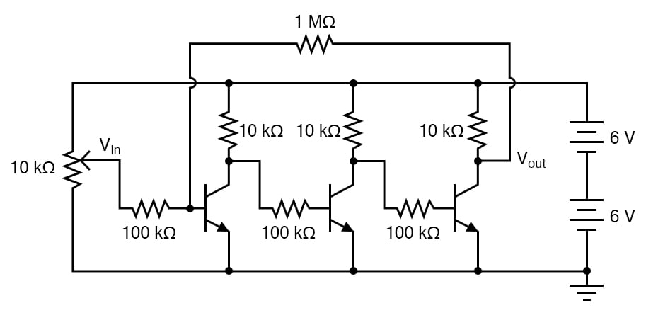
Figure 1. Schematic diagram of a multi-stage BJT common-emitter amplifier
The output of the first amplifier is the input of the second amplifier. Likewise, the output of the second amplifier is the input of the third amplifier. Also, notice how the 1 MΩ resistor provides negative feedback from the output of the third stage back to the input of the first stage.
Parts and Materials
- Three NPN transistors—model 2N2222 or 2N3403 recommended
- Two 6 V batteries
- One 10 kΩ potentiometer, single-turn, linear taper
- One 1 MΩ resistor
- Three 100 kΩ resistors
- Three 10 kΩ resistors
Learning Objectives
- Design of a multi-stage, direct-coupled common-emitter amplifier circuit
- Effect of negative feedback in an amplifier circuit
Instructions
Step 1: Connect three common-emitter amplifier circuits together, as illustrated in Figures 1 and 2, without the 1 MΩ feedback resistor, to begin with, to see for yourself just how high the unrestricted voltage gain is.
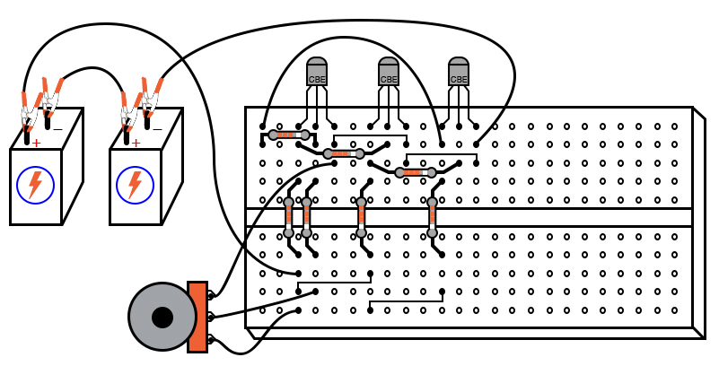
Figure 2. Breadboard implementation of the three-stage BJT common-emitter amplifier.
The collector terminal (output) of the previous transistor connects to the base resistor (input) of the next transistor.The voltage gains of each stage multiply together to give a high overall voltage gain:
$$G_{total} = G_1 \cdot G_2 \cdot G_3$$
Step 2: Try to adjust the potentiometer to calculate the gain. However, you may find it impossible to adjust the potentiometer for a stable output voltage (that isn’t saturated at full supply voltage or zero) because the gain is so high.
Step 3: Even if you can’t adjust the input voltage fine enough to stabilize the output voltage in the active range of the last transistor, you should be able to validate that the output-to-input relationship is inverting. That is to say, the output tends to drive to a high voltage when the input goes low, and vice versa. Since any one of the common-emitter stages is inverting in itself, an even number of staged common-emitter amplifiers gives a noninverting response, while an odd number of stages gives inverting.
Test these relationships by measuring the collector-to-ground voltage at each transistor while adjusting the input voltage potentiometer, noting whether or not the output voltage increases or decreases with an increase in input voltage.
Step 4: Connect the 1 MΩ feedback resistor to the circuit, coupling the collector of the last transistor to the base of the first. Since the overall response of this three-stage amplifier is inverting, the feedback signal provided through the 1 MΩ resistor from the output of the last transistor to the input of the first should be negative in nature. As such, it will act to stabilize the amplifier’s response and minimize the voltage gain.
Step 5: Adjust the potentiometer and measure the change in output voltage. You should notice the reduction in gain immediately by the decreased sensitivity of the output signal on input signal changes (changes in potentiometer position). Simply put, the amplifier isn’t nearly as touchy as it was without the feedback resistor in place. As with the earlier simple common-emitter amplifier experiment, it is a good idea here to make a table of input versus output voltage figures with which you may calculate voltage gain.
Step 6: Experiment with different values of feedback resistance. What effect do you think a decrease in feedback resistance has on voltage gain? What about an increase in feedback resistance? Try it by changing the feedback resistor value and find out!
An advantage of using negative feedback to tame a high-gain amplifier circuit is that the resulting voltage gain becomes more dependent upon the resistor values and less dependent upon the characteristics of the constituent transistors. This is good because it is far easier to manufacture consistent resistors than consistent transistors. Thus, it is easier to design an amplifier with predictable gain by building a staged network of transistors with an arbitrarily high voltage gain, then mitigate that gain precisely through negative feedback. It is this same principle that is used to make operational amplifier (op amp) circuits behave so predictably.
This amplifier circuit is a bit simplified from what you will normally encounter in practical multi-stage circuits. Rarely is a pure common-emitter configuration (i.e. with no emitter-to-ground resistor) used. Also, if the amplifier is being used for AC signals, the inter-stage coupling is often capacitive, with voltage divider networks connected to each transistor base for proper biasing of each stage.
Radio-frequency (RF) amplifier circuits are often transformer-coupled, with capacitors connected in parallel with the transformer windings for resonant tuning.
SPICE Simulation of a Multi-stage BJT Common-emitter Amplifier
Figure 3 is the three-stage BJT common-emitter amplifier circuit with node numbers added for SPICE circuit simulation.
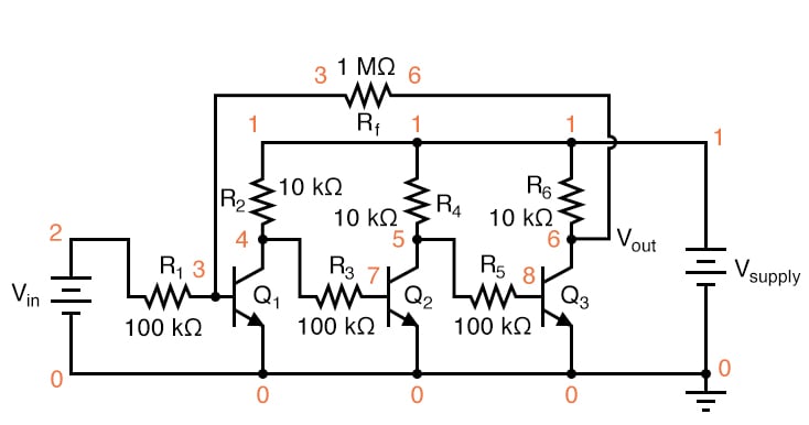
Figure 3. SPICE schematic of the three-stage BJT common-emitter amplifier.
The following netlist and input commands can be used to simulate the multi-stage common-emitter amplifier using SPICE.
Netlist (make a text file containing the following text, verbatim):
Multi-stage Common-emitter Amplifier
vsupply 1 0 dc 12
vin 2 0
r1 2 3 100k
r2 1 4 10k
q1 4 3 0 mod1
r3 4 7 100k
r4 1 5 10k
q2 5 7 0 mod1
r5 5 8 100k
r6 1 6 10k
q3 6 8 0 mod1
rf 3 6 1meg
.model mod1 npn bf=200
.dc vin 0 2.5 0.1
.plot dc v(6,0) v(2,0)
.end
This simulation plots output voltage against input voltage and allows comparison between those variables in numerical form, a list of voltage figures printed to the left of the plot. You may calculate voltage gain by taking any two analysis points and dividing the difference in output voltages by the difference in input voltages, just like you do for the real circuit.
Experiment with different feedback resistance values (rf) and see the impact on overall voltage gain. Do you notice a pattern?
Here’s a hint: the overall voltage gain may be closely approximated by using the resistance figures of r1 and rf without reference to any other circuit component!
Related Content
Learn more about the fundamentals behind this project in the resources below.
Textbook:
Worksheets:
- Class A BJT Amplifiers Worksheet
- Bipolar Junction Transistor (BJT) Theory Worksheet
- BJT Amplifier Troubleshooting Worksheet
- Multi-Stage Transistor Amplifiers Worksheet


Would R3 and R5 between transistors not actually override the amplification gained over the stages because it would limit the AC gain as much as DC?