Facebook
 Google
 GitHub
 Linkedin
Si Lab - BJT Common-emitter Amplifier
Project Overview
The common-emitter amplifier circuit illustrated in Figure 1 is one of the most important analog transistor circuits.
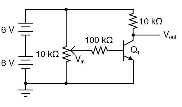
Figure 1. Schematic diagram of a BJT common-emitter amplifier circuit with potentiometer input control.
In this project, learn how to calculate amplifier voltage gain, be introduced to the difference between an inverting and a noninverting amplifier, and evaluate two different methods for adding negative feedback to this amplifier circuit.
Parts and Materials
- One NPN transistor—model 2N2222 or 2N3403 recommended
- Two 6 V batteries
- One 10 kΩ potentiometer, single-turn, linear taper
- One 1 MΩ resistor
- One 100 kΩ resistor
- One 10 kΩ resistor
- One 1.5 kΩ resistor
Learning Objectives
- Design of a simple common-emitter amplifier circuit
- How to measure the amplifier's voltage gain
- The difference between an inverting and a noninverting amplifier
- Ways to introduce negative feedback in an amplifier circuit
Instructions
Step 1: Build the common-emitter amplifier circuit shown in the schematic of Figure 1 and illustrated in Figure 2.
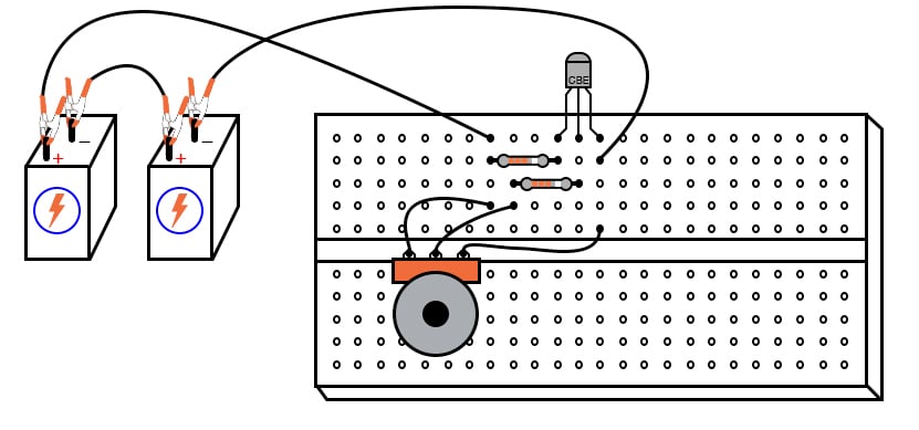
Figure 2. Breadboard implementation of a BJT common-emitter amplifier circuit with potentiometer input control.
Step 2: Measure the output voltage (voltage measured between the transistor’s collector terminal and ground) and the input voltage (voltage measured between the potentiometer’s wiper terminal and ground) for several position settings of the potentiometer. I recommend determining the output voltage range as the potentiometer is adjusted through its entire range of motion, then choosing several voltages spanning that output range to take measurements at.
For example, if full rotation on the potentiometer drives the amplifier circuit’s output voltage from 0.1 V (low) to 11.7 V (high), choose several voltage levels between those limits (1, 3, 5, 7, 9, and 11 V). Measuring the output voltage with a meter, adjust the potentiometer to obtain each of these predetermined voltages at the output, noting the exact figure for later reference.
Then, measure the exact input voltage producing that output voltage, and record that voltage figure as well. In the end, you should have a table of numbers representing several different output voltages along with their corresponding input voltages.
Step 3: Calculate the voltage gain using any two pairs of input and output voltages—divide the difference in output voltages by the difference in input voltages:
$$Gain = \frac{\Delta V_{OUT}}{\Delta V_{IN}} = \frac{V_{OUT2} - V_{OUT1}}{V_{IN2} - V_{IN1}}$$
For example, if an input voltage of 1.5 V gives me an output voltage of 7.0 V and an input voltage of 1.66 V gives me an output voltage of 1.0 V, the amplifier’s voltage gain is:
$$Gain = \frac{V_{OUT2} - V_{OUT1}}{V_{IN2} - V_{IN1}} = \frac{7.0 - 1.0}{1.5-1.66} = -37.5$$
You should immediately notice two characteristics while taking these voltage measurements:
- The input-to-output effect is reversed. That is, an increasing input voltage results in a decreasing output voltage. This effect is known as signal inversion, and this kind of amplifier is an inverting amplifier.
- This amplifier exhibits a strong voltage gain. A small change in input voltage results in a large change in output voltage. This should stand in stark contrast to the voltage follower amplifier circuit discussed earlier, which had a voltage gain of about 1.
Common-emitter amplifiers are widely used due to their high voltage gain, but they are rarely used in as crude a form as this. Although this amplifier circuit works to demonstrate the basic concept, it is very susceptible to changes in temperature.
Step 4: Try leaving the potentiometer in one position and heating the transistor by grasping it firmly with your hand or heating it with some other source of heat, such as an electric hair dryer. WARNING: be careful not to get it so hot that your plastic breadboard melts!
Step 5: You may also explore temperature effects by cooling the transistor. Touch an ice cube to its surface and note the change in output voltage. When the transistor’s temperature changes, its base-emitter diode characteristics change, resulting in different amounts of base current for the same input voltage. This, in turn, alters the controlled current through the collector terminal, thus affecting output voltage.
Using Feedback in Amplifier Circuits
Changes caused by temperature may be minimized through the use of signal feedback, whereby a portion of the output voltage is fed back to the amplifier’s input so as to have a negative, or canceling, effect on voltage gain. The temperature stability is improved at the expense of voltage gain; a compromise solution, but practical nonetheless.
Step 6: Perhaps the simplest way to add negative feedback to a common-emitter amplifier is to add some resistance between the emitter terminal and ground so that the input voltage becomes divided between the base-emitter PN junction and the voltage drop across the new resistance. Add the 1.5 kΩ resistor between the emitter and ground to the circuit, as illustrated in Figures 3 and 4.
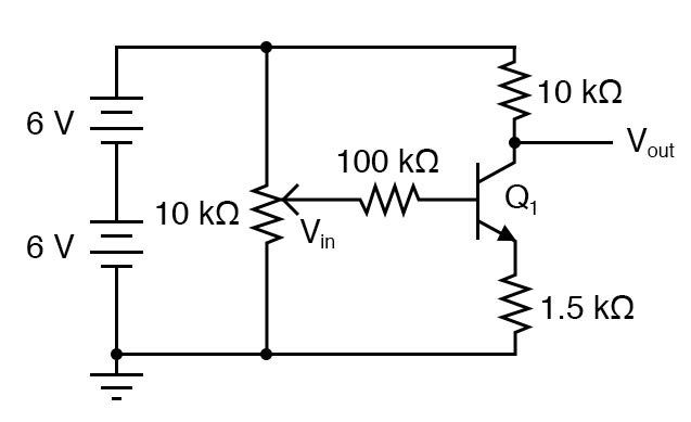
Figure 3. Schematic diagram of a BJT common-emitter amplifier with added resistance at the emitter node.
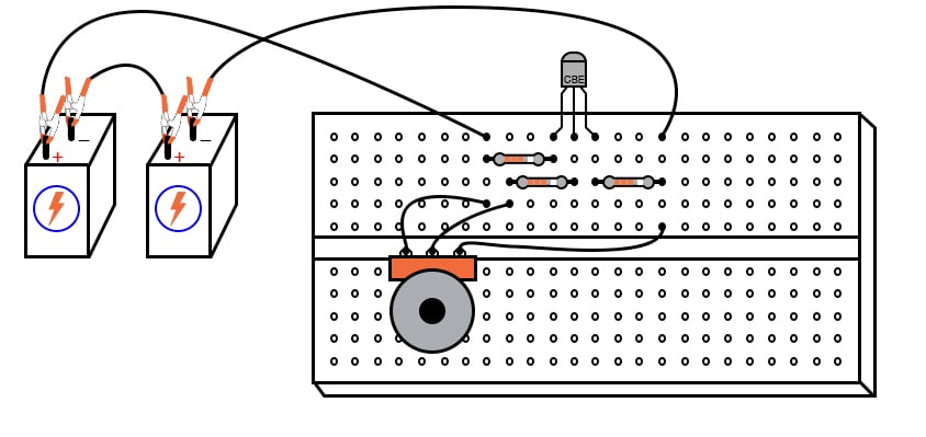
Figure 4. Breadboard implementation of a BJT common-emitter amplifier with added resistance at the emitter node.
Step 7: Repeat the same voltage measurement and recording exercise with the 1.5 kΩ resistor installed.
Step 8: Calculate the new (reduced) voltage gain of this circuit.
Step 9: Try altering the transistor’s temperature again and noting the output voltage for a steady input voltage. Does it change more or less than without the 1.5 kΩ resistor?
Step 10: Another method of introducing negative feedback to this amplifier circuit is to couple the output to the input through a high-value resistor. Connect a 1 MΩ resistor between the transistor’s collector and base terminals, as illustrated in Figures 5 and 6.
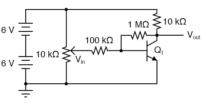
Figure 5. Schematic diagram of a BJT common-emitter amplifier with collector-base resistive feedback.
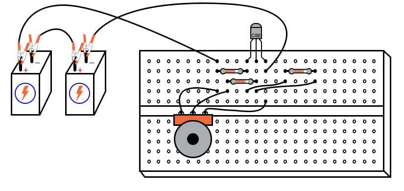
Figure 6. Breadboard implementation of a BJT common-emitter amplifier with collector-base resistive feedback.
Step 11: Calculate the voltage gain of this new circuit and evaluate the temperature response. Although this different method of feedback accomplishes the same goal of increased stability by diminishing gain, the two feedback circuits will not behave identically.
Step 12: Measure the range of possible output voltages with each feedback scheme (the low and high voltage values obtained with a full sweep of the input voltage potentiometer) and how this differs between the two circuits.
SPICE Simulation of a BJT Common-emitter Amplifier
To simulate the BJT voltage follower circuit, we can use the circuit shown in Figure 7 and the associated SPICE simulation netlist and input deck that follows.
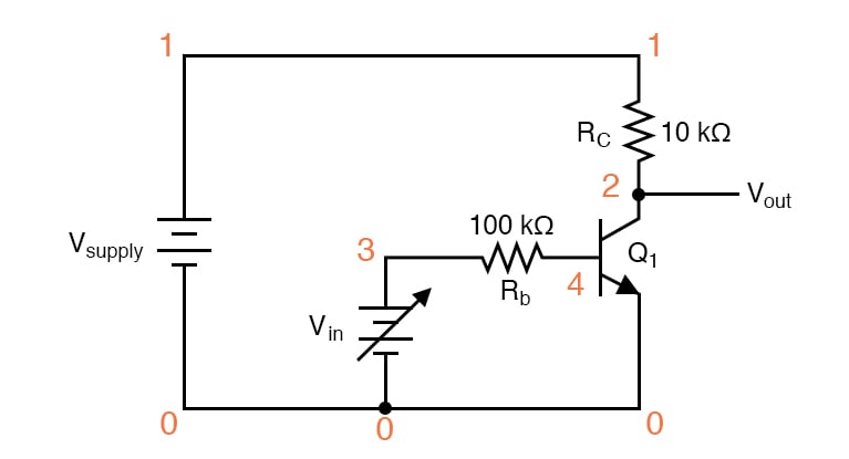
Figure 7. BJT common-emitter amplifier schematic for SPICE simulation.
Netlist (make a text file containing the following text, verbatim):
Common-emitter amplifier
vsupply 1 0 dc 12
vin 3 0
rc 1 2 10k
rb 3 4 100k
q1 2 4 0 mod1
.model mod1 npn bf=200
.dc vin 0 2 0.05
.plot dc v(2,0) v(3,0)
.end
This SPICE simulation sets up a circuit with a variable DC voltage source (vin) as the input signal and measures the corresponding output voltage between nodes 2 and 0. The input voltage is varied, or swept, from 0 to 2 V in 0.05 V increments.
The results are shown on a plot, with the input voltage appearing as a straight, increasing line. Due to the high gain of the amplifier, the output voltage will be a step function—beginning high and ending low, with a steep change in the middle where the transistor is in its active mode of operation.
Related Content
Learn more about the fundamentals behind this project in the resources below.
Textbook:
Worksheets:
- Bipolar Transistor Biasing Circuits Worksheet
- Class A BJT Amplifiers Worksheet
- Bipolar Junction Transistor (BJT) Theory Worksheet