Facebook
 Google
 GitHub
 Linkedin
Si Lab - Differential Amplifier
Project Overview
The differential amplifier circuit forms the heart of most op amp circuits. As illustrated in Figure 1, the transistor pair, Q1 and Q2, share a common emitter node that is connected to the 1.5 kΩ resistor.
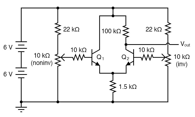
Figure 1. Schematic diagram of a BJT differential amplifier.
The two transistors form a differential pair. In the form shown here, it is a rather crude differential amplifier. The output voltage is quite nonlinear and unsymmetrical with regard to the input voltages.
Parts and Materials
- Two 6-volt batteries
- Two NPN transistors—models 2N2222 or 2N3403 recommended
- Two 10 kΩ potentiometers, single-turn, linear taper
- Two 22 kΩ resistors
- Two 10 kΩ resistors
- One 100 kΩ resistor
- One 1.5 kΩ resistor
Resistor values are not especially critical in this experiment but have been chosen to provide high voltage gain for a comparator-like differential amplifier behavior.
Learning Objectives
- The basic design of a differential amplifier circuit
- Working definitions of differential and common-mode voltages
Instructions
Step 1: Build the differential amplifier shown in the circuit schematic of Figure 1 and the breadboard implementation of Figure 2.
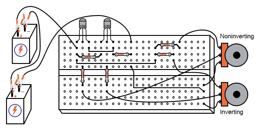
Figure 2. Breadboard implementation of a BJT differential amplifier.
Step 2: Using the left potentiometer in Figure 1, set the input voltage to the base of transistor Q1 to 2.5 V.
Step 3: Using the right potentiometer, set the initial input voltage to transistor Q2 to 2.0 V. Measure the output voltage at the collector of Q2 with respect to the ground.
Step 4: Slowly sweep the input voltage to the transistor, Q2, while monitoring the output voltage. With a high voltage gain created by a large collector/emitter resistor ratio (100 kΩ/1.5 kΩ), though, it acts primarily as a comparator, where the output voltage rapidly changes value as the two input voltage signals approach equality.
Step 4: Now, using the right potentiometer in Figure 1, set the input voltage to the base of transistor Q2 to 2.5 V.
Step 5: Using the left potentiometer, set the initial input voltage to transistor Q1 to 2.0 V. Measure the output voltage at the collector of Q2 with respect to the ground.
Step 6: Slowly sweep the input voltage to transistor Q1 while monitoring the output voltage. Note how the two potentiometers have different effects on the output voltage. The input to the transistor, Q1 (V+), tends to drive the output voltage in the same direction (noninverting), while the input to the transistor, Q2 (V-), tends to drive the output voltage in the opposite direction (inverting). This is the essential nature of a differential amplifier—it amplifies the difference between the two inputs, including the sign:
$$V_{out} = Gain \cdot (V_{+} - V_{-})$$
Ideally, the output voltage of such an amplifier is strictly a function of the difference between the two input signals. This circuit falls considerably short of the ideal, as even a cursory test will reveal.
Common-mode Voltage
An ideal differential amplifier ignores all common-mode voltage, which is whatever level of voltage common to both inputs. For example, if the inverting input is at 3.0 V and the noninverting input is at 2.5 V, the differential voltage will be 0.5 V (3 - 2.5), but the common-mode voltage will be 2.5 V since that is the lowest input signal level. Ideally, this condition should produce the same output signal voltage as if the inputs were set at 3.5 and 3 V, respectively (0.5 V differential, with a 3 V common-mode voltage).
Step 7: Repeat steps 2-4 above, but with the input of Q1 at 3.5 V and Q2 beginning at 3.0 V. This circuit does not give the same result for the two different input signal scenarios. In other words, its output voltage depends on both the differential voltage and the common-mode voltage.
As imperfect as this differential amplifier is, its behavior could be worse. Note how the input signal potentiometers have been limited by 22 kΩ resistors to an adjustable range of approximately 0 to 4 V, given a power supply voltage of 12 volts.
Step 8: If you’d like to see how this circuit behaves without any input signal limiting, just bypass the 22 kΩ resistors with jumper wires, allowing a full 0 to 12 V adjustment range from each potentiometer. Do not worry about building up excessive heat while adjusting potentiometers in this circuit. Unlike the current mirror circuit, this circuit is protected from thermal runaway by the emitter resistor (1.5 kΩ), which doesn’t allow enough transistor current to cause any problem.
Related Content
Learn more about the fundamentals behind this project in the resources below.
Textbook:
Worksheets:
- Bipolar Transistor Biasing Circuits Worksheet
- Bipolar Junction Transistor (BJT) Theory Worksheet
- Differential Transistor Amplifiers Worksheet