Facebook
 Google
 GitHub
 Linkedin
Si Lab - BJT Common-collector Voltage Follower
Project Overview
In this project, you will construct the voltage follower circuit using a bipolar transistor, as illustrated in Figure 1.
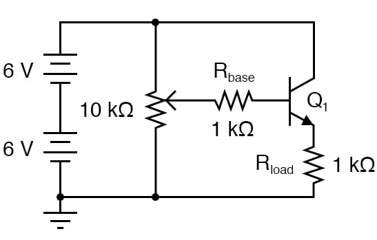
Figure 1. Schematic diagram of a BJT emitter-follower circuit with potentiometer input control.
The voltage follower is the safest and easiest transistor amplifier circuit to build. Its purpose is to provide approximately the same voltage to the load as what is input to the amplifier but at a much greater current. In other words, it has no voltage gain, but it does have a current gain. This configuration is also called a common-collector amplifier because the collector of the BJT is connected to a power supply.
Parts and Materials
- One NPN transistor—models 2N2222 or 2N3403 recommended
- Two 6 V batteries
- Two 1 kΩ resistors
- One 10 kΩ potentiometer, single-turn, linear taper
Beware that not all transistors share the same terminal designations, or pinouts, even if they share the same physical appearance. This will dictate how you connect the transistors together and to other components, so be sure to check the manufacturer’s specifications (component datasheet), easily obtained from the manufacturer’s website.
Another thing to keep in mind is that it is possible for the transistor’s package and even the manufacturer’s datasheet to show incorrect terminal identification diagrams! Double-checking pin identities with your multimeter’s diode check function is highly recommended. For details on how to identify bipolar transistor terminals using a multimeter, consult the textbook page, Meter Check of a Transistor (BJT),
Learning Objectives
- Purpose of circuit ground when there is no actual connection to earth ground
- Using a shunt resistor to measure current with a voltmeter
- Measure amplifier voltage gain
- Measure amplifier current gain
- Amplifier impedance transformation
Instructions
Step 1: Build the circuit shown in the schematic of Figure 1 and illustrated in Figure 2.
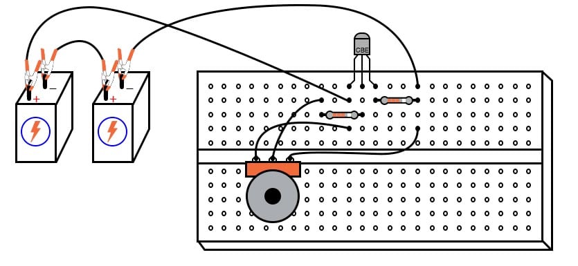
Figure 2. Breadboard implementation of a BJT emitter-follower circuit with potentiometer input control.
Again, beware that the transistor you select for this experiment may not have the same terminal designations shown here, and so the breadboard layout shown in the illustration may not be correct for you. In the illustrations, all TO-92 package transistors have terminals labeled “CBE” (collector, base, and emitter) from left to right. This is correct for the model 2N2222 transistor and some others, but not for all; not even for all NPN-type transistors. As usual, check with the manufacturer for details on the particular component(s) you choose for a project.
Understanding Circuit Ground
Note that the negative (-) side of the power supply is shown in the schematic diagram of Figure 1 to be connected to the ground, as indicated by the symbol in the lower-left corner of the diagram. This does not necessarily represent a connection to the actual earth. What it means is that this point in the circuit—and all points electrically common to it, as shown in Figure 3—constitutes the default reference point for all voltage measurements in the circuit.
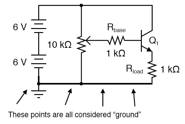
Figure 3. Circuit ground is the default reference node for a circuit.
Since the voltage is by necessity a quantity relative between two points, a “common” point of reference designated in a circuit gives us the ability to speak meaningfully of voltage at particular, single points in that circuit. For example, if we were to take the voltage at the base of the transistor (VB), it would mean the voltage measured between the transistor’s base terminal and the negative side of the power supply (ground). This is demonstrated in Figure 4, with the red probe touching the base terminal and the black probe touching the ground.
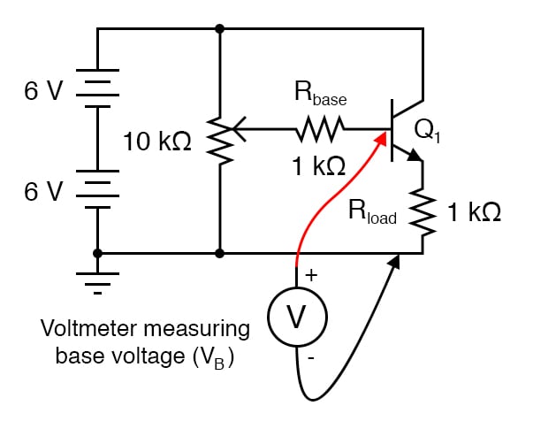
Figure 4. Node voltages, like VB, are assumed to be referenced to circuit ground.
Normally, it is nonsense to speak of voltage at a single point, but having an implicit reference point (ground) for voltage measurements makes such statements meaningful.
Step 2: Measure the output voltage versus input voltage for several different potentiometer settings. The output voltage is the voltage across the load resistor voltage (or the emitter voltage between the emitter and circuit ground). The input voltage is the voltage at the potentiometer’s wiper (voltage between the wiper and circuit ground).
You should see a close correlation between these two voltages: one is just a little bit greater than the other (about 0.6 V or so). However, a change in the input voltage gives an almost equal change in the output voltage. The output follows the input, which is why it is called a voltage follower.
Step 3: Since the relationship between input change and output change is almost 1:1, we can say that the AC voltage gain of this amplifier is nearly 1. Not very impressive, is it? Now measure the current through the base of the transistor (input current) versus the current through the load resistor (output current). Before you break the circuit and insert your ammeter to take these measurements, consider an alternative method: measure the voltage across the base and load resistors, whose resistance values are known.
Using Ohm’s Law, the current through each resistor may be easily calculated: divide the measured voltage by the known resistance (I = V/R). This calculation is particularly easy with resistors of 1 kΩ value: there will be 1 mA of current for every 1 volt of drop across them.
Step 4: For best precision, you may measure the resistance of each resistor rather than assume an exact value of 1 kΩ, but it really doesn’t matter much for the purposes of this experiment. When resistors are used to take current measurements by translating a current into a corresponding voltage, they are often referred to as shunt resistors.
You should expect to find huge differences between input and output currents for this amplifier circuit. In fact, it is not uncommon to experience current gains well in excess of 200 for a small-signal transistor operating at low current levels. This is the primary purpose of a voltage follower circuit: to boost the current capacity of a weak signal without altering its voltage.
Another way of thinking of this circuit’s function is in terms of impedance. The input side of this amplifier accepts a voltage signal without drawing much current. The output side of this amplifier delivers the same voltage but at a current limited only by load resistance and the current-handling ability of the transistor. Cast in terms of impedance, we could say that this amplifier has a high input impedance (voltage dropped with the little current drawn) and a low output impedance (voltage dropped with almost unlimited current-sourcing capacity).
SPICE Simulation of the BJT Emitter Follower Circuit
To simulate the BJT voltage follower circuit, we can add node numbers to the schematic diagram, as shown in Figure 5, and use the SPICE simulation netlist and input deck that follows.
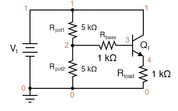
Figure 5. Adding node numbers to the emitter follower amplifier for SPICE simulation.
Netlist (make a text file containing the following text, verbatim):
BJT Voltage Follower
v1 1 0
rpot1 1 2 5k
rpot2 2 0 5k
rbase 2 3 1k
rload 4 0 1k
q1 1 3 4 mod1
.model mod1 npn bf=200
.dc v1 12 12 1
.print dc v(2,0) v(4,0) v(2,3)
.end
When this simulation is run through the SPICE program, it shows an input voltage of 5.937 V and an output voltage of 5.095 V, with an input current of 25.35 µA (2.535E-02 V dropped across the 1 kΩ Rbase resistor). Output current is, of course, 5.095 mA, inferred from the output voltage of 5.095 V dropped across a load resistance of exactly 1 kΩ.
You may change the input voltage of this circuit by adjusting the values of Rpot1 and Rpot2, always keeping their sum at 10 kΩ.
Related Content
Learn more about the fundamentals behind this project in the resources below.
Textbook:
Worksheets:
- Bipolar Transistor Biasing Circuits Worksheet
- Bipolar Junction Transistor (BJT) Theory Worksheet
- Ohm's Law Worksheet