Facebook
 Google
 GitHub
 Linkedin
Analog Lab - Non-inverting Amplifier
Project Overview
The non-inverting amplifier with an adjustable gain is one of the most useful circuits you can build with an operational amplifier (op amp). As illustrated in Figure 1, the op amp uses a resistor divider (potentiometer, R2) to provide negative feedback.
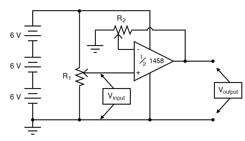
Figure 1. Schematic diagram of the op amp non-inverting amplifier circuit.
As we will demonstrate, this divided negative feedback is key to the operation of the non-inverting amplifier.
Parts and Materials
- Op amp, model 1458 or 353, recommended
- Three 6 V batteries or an 18 V power supply
- Two 10 kΩ potentiometers, linear taper
Learning Objectives
- How to use an op amp as a single-ended amplifier
- How to use divided negative feedback
Theory of Operation
This circuit differs from the voltage follower project in only one respect, the output voltage is fed back to the inverting (-) input through a voltage-dividing potentiometer rather than being directly connected. With only a fraction of the output voltage fed back to the inverting input, the op amp will output a corresponding multiple of the voltage sensed at the noninverting (+) input to keep the input differential voltage near zero.
In other words, the op amp will now function as an amplifier with a controllable voltage gain, that gain is established by the position of the feedback potentiometer (R2).
Instructions
Step 1: Build the non-inverting amplifier circuit of Figure 1. A breadboard implementation of this circuit is illustrated in Figure 2.
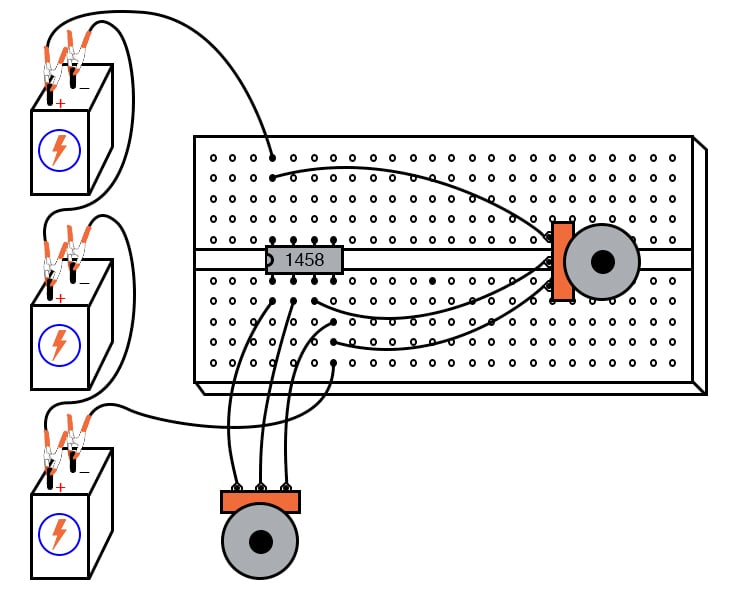
Figure 2. Breadboard implementation of the op amp non-inverting amplifier.
Step 2: Set R2 to approximately mid-position. This should give a voltage gain of about 2. See the derivation of the non-inverting amplifier gain equation (which is discussed later in this chapter) to understand why this is true.
Step 3: Measure both the input and output voltage for several positions of the input potentiometer R1.
Step 4: Move R2 to a different position and re-take voltage measurements for several positions of R1. For any given R2 position, the ratio between output and input voltage should be the same. The ability to leverage an op amp in this fashion to create an amplifier with controllable voltage gain makes this circuit an extremely useful one.
You will also notice that the input and output voltages are always positive with respect to the ground. Since the output voltage increases in a positive direction for a positive increase of the input voltage, this amplifier is referred to as non-inverting. If the output and input voltages were related to one another in an inverse fashion (i.e. positive increasing input voltage results in positive decreasing or negative increasing output), then the amplifier would be known as an inverting type.
Step 5: Try adjusting R2 for maximum and minimum voltage gain. What is the minimum voltage gain attainable with this amplifier configuration? Why do you think this is?
Op Amp Non-inverting Amplifier Gain Equation
Let's derive the non-inverting amplifier gain equation using the schematic of Figure 3, which has distinct resistors, R1 and R2, in the negative feedback path.
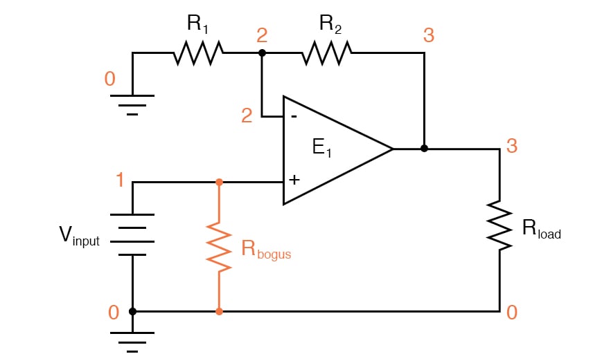
Figure 3. SPICE circuit schematic with node numbers for simulation of the op amp non-inverting amplifier
Beginning from the op amp open-loop gain equation:
$$V_{out} = A \cdot (V_+ - V_-) = A \cdot (V_{in} - V_-)$$
Where A is the open-loop gain of the op amp, and we are defining the non-inverting op amp input (V+) as the non-inverting amplifier input, Vin.
The relationship of V- to Vout is given by the resistive voltage divider equation:
$$V_{-} = \left( \frac{R_1}{R_1+R_2} \right) V_{out}$$
Substituting, we get:
$$V_{out} = A\left(V_{in} - \left( \frac{R_1}{R_1+R_2} \right) V_{out} \right)$$
$$V_{out} + A\left( \frac{R_1}{R_1+R_2} \right) V_{out} = AV_{in}$$
Dividing both sides of the equation by the open-loop op amp gain, A, results in:
$$V_{out} \left( 1 + A\left( \frac{R_1}{R_1+R_2} \right) \right) = AV_{in}$$
Now, we will make an approximation to simplify the remaining analysis. The op amp open-loop gain, A, is typically a very large number, at least 10,000, and often much more. So, we will make the following approximation:
$$\frac{1}{A} \approx 0$$
This reduces our equation to:
$$V_{out} \left( \frac{R_1}{R_1+R_2}\right) = V_{in}$$
With some simple rearranging of terms, we arrive at our non-inverting amplifier gain, G:
$$G = \frac{V_{out}}{V_{in}} = 1 + \frac{R_2}{R_1}$$
SPICE Simulation of the Non-inverting Amplifier
The circuit schematic of Figure 3 uses a dependent voltage source (E1) to simulate an op amp.
Netlist (make a text file containing the following text, verbatim):
Noninverting amplifier
vinput 1 0
r2 3 2 5k
r1 2 0 5k
rbogus 1 0 1meg
e1 3 0 1 2 999meg
rload 3 0 10k
.dc vinput 5 5 1
.print dc v(1,0) v(3,0)
.end
With R1 and R2 set equally to 5 kΩ in the simulation, it mimics the feedback potentiometer of the real circuit at mid-position (50%). To simulate the potentiometer at the 75% position, set R2 to 7.5 kΩ and R1 to 2.5 kΩ.
Related Content
Learn more about the fundamentals behind this project in the resources below.
Calculators:
- Op Amp Voltage and Gain Calculator
- Inverting Op Amp Resistor Calculator
- Non-inverting Op Amp Resistor Calculator
- Voltage Divider Calculator
Textbook:
Worksheet:
- Inverting and Non-inverting Op Amp Voltage Amplifier Circuits Worksheet
- Basic Operational Amplifier Worksheet
- Op Amp Circuits Worksheet