 Facebook
 Google
 GitHub
 Linkedin
Analog Lab - Op Amp Integrator
Project Overview
Integrator circuits are one of the fundamental building-block functions of an analog computer. By connecting integrator circuits with amplifiers, summers, and potentiometers (dividers), almost any differential equation could be modeled, and solutions obtained by measuring voltages produced at various points in the network of circuits.
Since differential equations describe so many physical processes, analog computers are often used as physical simulators. Before the advent of modern digital computers, engineers used analog computers to simulate such processes as machinery vibration, rocket trajectory, and control system response. Even though analog computers are largely considered obsolete by modern standards, the integrator circuit can still be used in analog systems.
In this project, you will build the operational amplifier (op amp) integrator circuit of Figure 1 that includes a capacitor in the negative feedback path from the output to the inverting input.
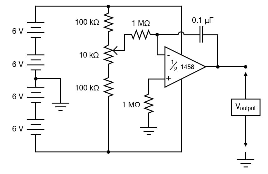
Figure 1. Schematic diagram of the op amp integrator circuit.
Parts and Materials
- Four 6 V batteries or 24 V power supply
- Operational amplifier, model 1458 recommended
- One 10 kΩ potentiometer, linear taper
- Two capacitors, 0.1 µF each, non-polarized
- Two 100 kΩ resistors
- Three 1 MΩ resistors
Just about any op amp model will work fine for this integrator experiment, but I’m specifying the model 1458 over the 353 because the 1458 has much higher input bias currents. Normally, a high input bias current is a bad characteristic for an op amp to have in a precision DC amplifier circuit (and especially an integrator circuit). However, I want the bias current to be high in order that its bad effects may be exaggerated and so that you will learn one method of counteracting its effects.
Learning Objectives
- To show a method for limiting the span of a potentiometer
- To determine the purpose of an integrator circuit
- To illustrate how to compensate for op amp bias current
Instructions
Step 1: Build the circuit shown in the schematic diagram of Figure 1 and illustrated in the breadboard implementation of Figure 2.
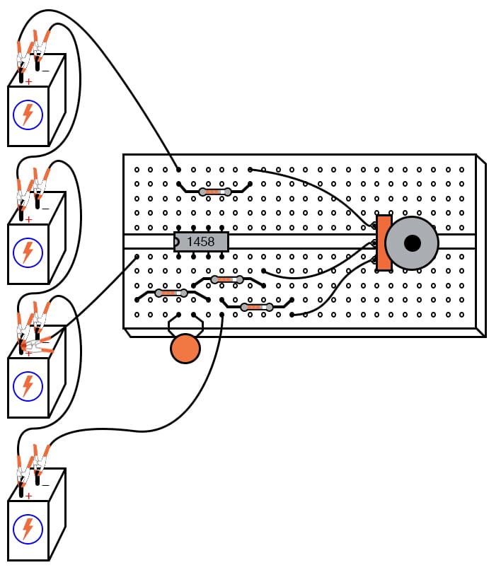
Figure 2. Breadboard implementation of the op amp integrator circuit.
As you can see from the schematic diagram, the 10 kΩ potentiometer is connected to 100 kΩ resistors, one on each end, that are then connected to the rails of the power supply. This is to limit the span of the potentiometer so that full movement produces a fairly small range of input voltages for the op amp to operate on.
At one extreme of the potentiometer’s motion, a voltage of about 0.5 volts (with respect to the ground point in the middle of the series battery string) will be produced at the potentiometer wiper. At the other extreme of motion, a voltage of about -0.5 volts will be produced. When the potentiometer is positioned dead-center, the wiper voltage should measure zero volts.
Step 2: Connect a voltmeter between the op amp’s output terminal and the circuit ground point. Slowly move the potentiometer control while monitoring the output voltage. The output voltage should change at a rate established by the potentiometer’s deviation from the zero (center) position.
To use calculus terms, we would say that the output voltage represents the integral (with respect to time) of the input voltage function. That is, the input voltage level establishes the output voltage rate of change over time.
This is precisely the opposite of differentiation, where the derivative of a signal or function is its instantaneous rate of change.
Step 3: If you have two voltmeters, you may readily see this relationship between the input voltage and output voltage rate of change by measuring the wiper voltage (between the potentiometer wiper and ground) with one meter and the output voltage (between the op amp output terminal and ground) with the other.
Adjusting the potentiometer to give zero volts should result in the lowest output voltage rate of change. Conversely, the more voltage input to this circuit, the faster its output voltage will change, or ramp rate.
Step 4: Connect the second 0.1 µF capacitor in parallel with the first. This will double the amount of capacitance in the op amp’s feedback loop. What effect does this have on the circuit’s integration rate for any given potentiometer position?
Step 5: Connect another 1 MΩ resistor in parallel with the input resistor (the resistor connecting the potentiometer wiper to the inverting terminal of the op amp). This will be half the integrator’s input resistance. What effect does this have on the circuit’s integration rate?
Step 6: Move the potentiometer until the op amp’s output voltage is as close to zero as you can get it, and move as slowly as you can make it.
Step 7: Disconnect the integrator input from the potentiometer wiper terminal and connect it instead to the ground, as illustrated in Figures 3 and 4.
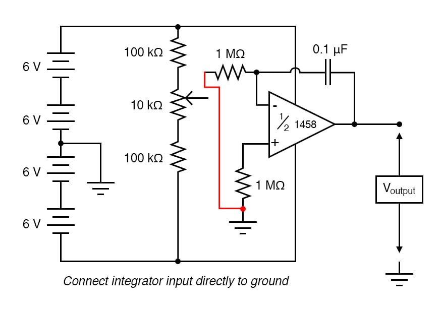
Figure 3. Schematic diagram of the op amp integrator circuit with integrator input grounded.
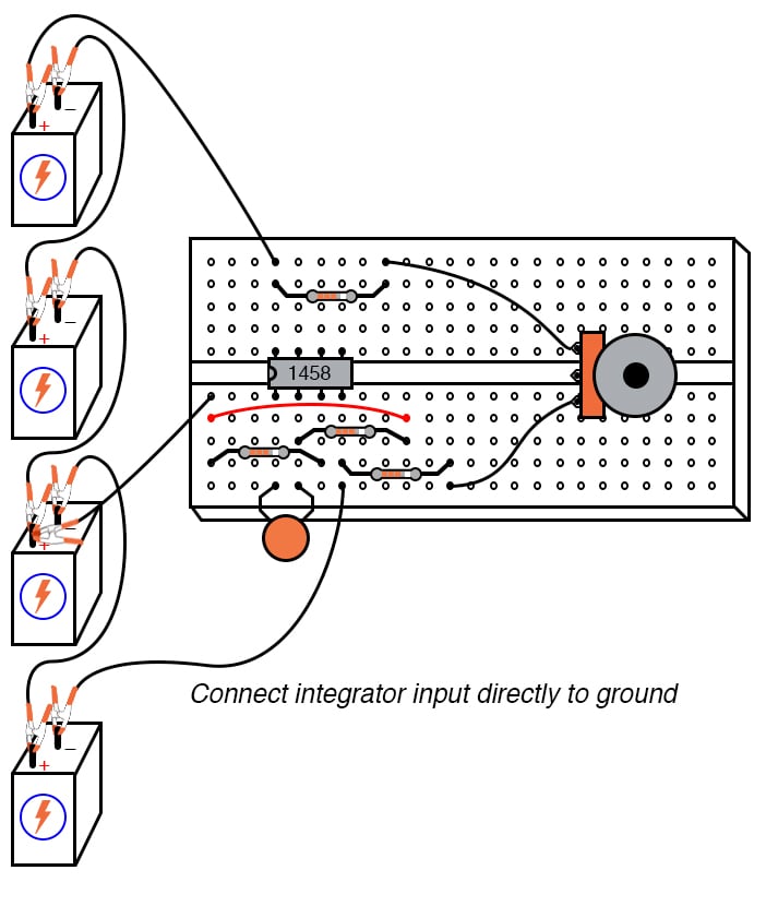
Figure 4. Breadboard implementation of the op amp integrator circuit with integrator input grounded.
Applying exactly zero voltage to the input of an integrator circuit should, ideally, cause the output voltage rate-of-change to be zero. When you make this change to the circuit, you should notice the output voltage remaining at a constant level or changing very slowly.
Step 8: With the integrator input still shorted to ground, short past the 1 MΩ resistor connecting the op amp’s noninverting (+) input to ground, as illustrated in Figures 5 and 6.
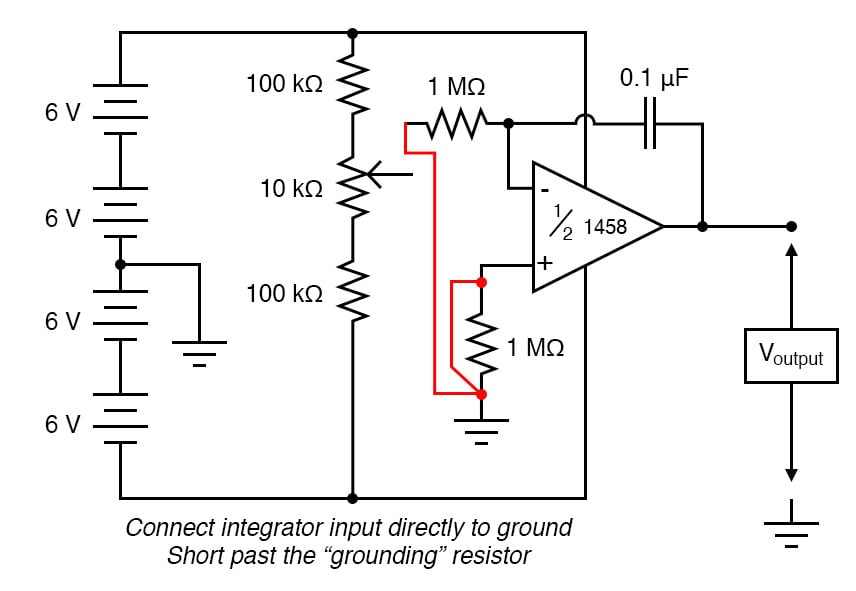
Figure 5. Schematic diagram of the op amp integrator circuit after shorting the grounding resistor
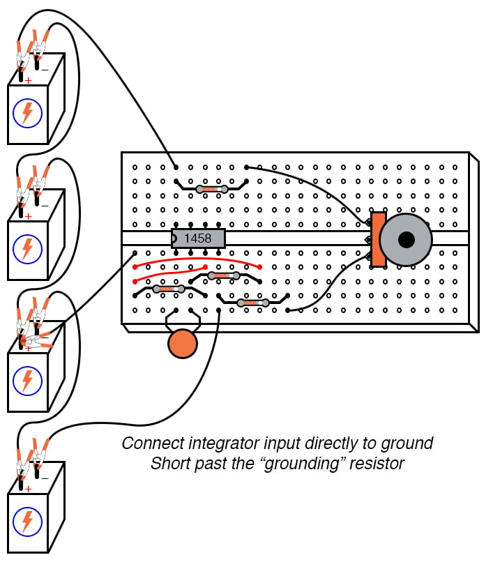
Figure 6. Breadboard implementation of the op amp integrator circuit after shorting the grounding resistor
There should be no need for this resistor in an ideal op amp circuit, so by shorting past it, we will see what function it provides in this very real op amp circuit.
Step 9: Next. measure the output voltage. As soon as the grounding resistor is shorted with a jumper wire, the op amp’s output voltage will start to change or drift. Ideally, this should not happen because the integrator circuit still has an input signal of zero volts. However, real operational amplifiers have a very small amount of current entering each input terminal called the bias current. These bias currents will drop voltage across any resistance in their path.
Since the 1 MΩ input resistor conducts some amount of bias current regardless of input signal magnitude, it will drop voltage across its terminals due to bias current, thus offsetting the amount of signal voltage seen at the inverting terminal of the op amp. If the other (non-inverting) input is connected directly to the ground, as we have done here, this offset voltage incurred by voltage drop generated by bias current will cause the integrator circuit to slowly integrate as though it were receiving a very small input signal.
The grounding resistor is better known as a compensating resistor because it compensates for voltage errors created by the bias current. Since the bias currents through each op amp input terminal are approximately equal to each other, an equal amount of resistance placed in the path of each bias current will produce approximately the same voltage drop. Equal voltage drops seen at the complementary inputs of an op amp cancel each other out, thus nulling the error otherwise induced by a bias current.
Step 10: Remove the jumper wire shorting past the compensating resistor and notice how the op amp output returns to a relatively stable state. It may still drift some, most likely due to bias voltage error in the op amp itself, but that is another subject altogether!
SPICE Simulation of the Op Amp Integrator Circuit
The circuit schematic of Figure 7 uses a dependent voltage source (E) to simulate an op amp.
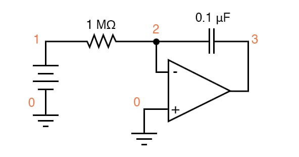
Figure 7. SPICE circuit schematic with node numbers for simulation of the op amp integrator.
Netlist (make a text file containing the following text, verbatim):
DC integrator
vinput 1 0 dc 0.05
r1 1 2 1meg
c1 2 3 0.1u ic=0
e1 3 0 0 2 999k
.tran 1 30 uic
.plot tran v(1,0) v(3,0)
.end
Related Content
Learn more about the fundamentals behind this project in the resources below.
Textbook:
Worksheets:
- Inverting and Non-inverting Op Amp Voltage Amplifier Circuits Worksheet
- Op Amp Circuits Worksheet
- Basic Operational Amplifiers Worksheet
- AC Negative Feedback Op Amp Circuits Worksheet
- Linear Computational Circuitry Worksheet


