Facebook
 Google
 GitHub
 Linkedin
Clean Clocking: The New CDCE813-Q1 Clock Synthesizer
The CDCE813-Q1 is a customizable, fairly high-frequency clock generator that is qualified for automotive applications.
Learn more about a new clocking generator in this tech brief on the CDCE813-Q1, a fairly high-frequency clock generator qualified for automotive applications.
Clock synthesis is perhaps not the most thrilling aspect of today’s digital and mixed-signal designs. But that doesn’t mean it’s not important. Some people design Mars rovers and some design homebrew bottle-capper gadgets—and I’d rather live without the rovers.
The fact is, a good digital design starts with good clocks. You can incorporate layer upon layer of complicated functionality, but if the timing signals driving all this functionality are excessively jittery or inaccurate in terms of frequency or highly susceptible to EMI, you’re going to have problems.
One of the issues that comes up in modern designs is the need for multiple clocks of different frequency. All you have to do is look at a Raspberry Pi 3 and think about the various clock signals that must be required for all that functionality—CPU, Wi-Fi, Bluetooth, Ethernet. . . .
Thus, it’s not surprising that semiconductor manufacturers offer clock-synthesis ICs. These components can generate multiple clocks of different frequency from a single reference clock and, as usual, you are likely to get plenty of other functionality to boot.
One In, Three Out
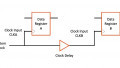
The CDCE813-Q1 accepts one input clock and generates three output clocks. Here is the block diagram:

All images courtesy of Texas Instruments
As you can see, the device is built around a phase-locked loop (PLL). Operation is controlled via the increasingly ubiquitous I2C protocol and, if you aren’t looking to maximize your data rate, you can even save yourself some trouble and use the internal 500 kΩ pull-up resistors.
The CDCE813-Q1 can generate an input clock from a crystal or you can use an LVCMOS logic signal. One handy feature is the integrated adjustable crystal load capacitors; you can see them in the above diagram as the capacitor symbols with the diagonal arrows.
For some reason, I am perpetually annoyed by the need to calculate the proper load capacitance for crystals, and then there is the accompanying apprehension about choosing the wrong value and being forced to break out my soldering iron. Internal and digitally adjustable—that’s my type of crystal load cap.
However, if you plan on using a crystal, don’t forget about the frequency restrictions. With an LVCMOS clock input, you can go up to 160 MHz, but the max frequency for a crystal-based input is 32 MHz.
Spreading the Spectrum
For those of you who are concerned about EMI performance, the CDCE813-Q1 offers a spread-spectrum clocking option. In systems that can tolerate small variations in clock frequency, this is a painless yet effective technique for facilitating EMI compliance.

And, actually, you can control the spread-spectrum behavior via digital input pins (i.e., no need for an I2C transaction). These user-programmable input signals can also be used to select different output frequencies, disable the outputs, and place the device in its power-down state.
Nonvolatility
I imagine that there are many applications that require the CDCE813-Q1’s versatility only for initial configuration—in other words, there will be no need to repeatedly change the device’s operational details. Systems such as these can benefit from the integrated nonvolatile memory: You write to the chip via I2C and then the internal register data can be transferred to the EEPROM. Now your custom configuration has become the power-up configuration.
Another handy feature is the CDCE813-Q1’s compatibility with TI’s Pro-Clock software. (Strangely, the datasheet refers to “Pro-Clock”— but if you look here, the software seems to be called “ClockPro”.) This software can help you optimize the register settings.
Clean Clocks, Clean Power
The CDCE813-Q1 is advertised as a “jitter cleaner”. (Is it just me, or is electronics terminology becoming increasingly awkward?) This refers to its ability to reduce the jitter in an incoming clock signal. Actually, the CDCE813-Q1’s default configuration is that of a “jitter cleaner”—i.e., the output frequency equals the input frequency, but jitter is reduced because the input signal passes through the PLL.

Good design practices become especially important when we’re dealing with high-speed signals (the CDCE813-Q1’s max output frequency is 230 MHz). This means, among other things, careful bypassing. As always, the reference design given in the datasheet is a very good place to start.

Notice the generous use of bypass caps, and also the ferrite beads for increased power-line noise suppression. (The components are labeled L1 and L2, but I’m assuming they’re actually beads, not inductors.)
Are there any new clock-synthesis or clock-distribution ICs that AAC readers should know about? Feel free to share your thoughts in the comments.