Facebook
 Google
 GitHub
 Linkedin
Considerations for FPGA Implementation of Linear-Phase FIR Filters
This article will review considerations for efficient FPGA implementation of symmetric FIR filters.
This article will review considerations for efficient FPGA implementation of symmetric FIR filters.
This article will derive a modular pipelined structure for symmetric FIR filters. We’ll see that the derived structure can be efficiently implemented using the DSP slices of the Xilinx FPGAs.
Symmetric FIR Filters
Let’s consider an eight-tap FIR filter. The transfer function of this filter will be
$$Y(z)= \sum_{k=0}^{7} z^{-k} h_k X(z)$$
Assume that the filter is symmetric and we have $$h_k = h_{7-k}$$ for $$k=0, 1, \dots ,7$$. Hence, the transfer function can be rewritten as
$$Y(z)= (1+z^{-7})h_0X(z)+(z^{-1}+z^{-6})h_1X(z)+(z^{-2}+z^{-5})h_2X(z)+ (z^{-3}+z^{-4})h_3X(z)$$
Equation 1
We can implement Equation 1 as a system with four levels of pipelining, as shown in Figure 1. Each stage of this block diagram corresponds to one of the four terms of Equation 1.
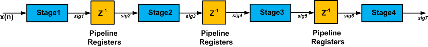
Figure 1. Click to enlarge.
Since we have inserted three register sets to perform pipelining, we expect a latency of three clock cycles. In terms of the z transformation, the output of Figure 1 will be $$z^{-3}$$ times $$Y(z)$$ (as given in Equation 1). In other words, we have $$sig7=z^{-3}Y(z)$$. Hence, we have
$$\begin{align}
sig7 &= z^{-3}(1+z^{-7})h_0X(z)
+z^{-3}(z^{-1}+z^{-6})h_1X(z) \\
&+z^{-3}(z^{-2}+z^{-5})h_2X(z) + z^{-3}(z^{-3}+z^{-4})h_3X(z)
\end{align}$$
Equation 2
Now, we should allocate each of these four terms to an appropriate stage in Figure 1. We have the equation for the output sig7, so it’s easier to first design the last stage of the system. If we implement the term $$z^{-3}(1+z^{-7})h_0X(z)$$ as Stage 4, we’ll have to cascade ten delay elements to implement $$z^{-10}$$. However, if we implement $$z^{-3}(z^{-3}+z^{-4})h_3X(z)$$ as Stage 4, we’ll need a cascade of only seven delay elements. Hence, we’ll implement the last term of Equation 2 as Stage 4 of Figure 1. This gives the circuit shown in Figure 2.

Figure 2
Therefore, we obtain
$$sig6 = z^{-3}(1+z^{-7})h_0X(z)
+z^{-3}(z^{-1}+z^{-6})h_1X(z)+z^{-3}(z^{-2}+z^{-5})h_2X(z)$$
which gives
$$sig5 = z^{-2}(1+z^{-7})h_0X(z)
+z^{-2}(z^{-1}+z^{-6})h_1X(z)+z^{-2}(z^{-2}+z^{-5})h_2X(z)$$
Now, just like Stage 4, we can derive Stage 3 of Figure 1 and obtain the circuit in Figure 3.

Figure 3
Now, we have
$$sig3 = z^{-1}(1+z^{-7})h_0X(z)
+z^{-1}(z^{-1}+z^{-6})h_1X(z)$$
which can be rewritten as
$$sig3 = z^{-1}sig1
+z^{-1}(z^{-1}+z^{-6})h_1X(z)$$
where
$$sig1 = (1+z^{-7})h_0X(z)$$
Using these two equations, we can find the final structure shown in Figure 4.

Figure 4. Click to enlarge.
Note that for the first stage, an adder with a zero input is included to emphasize the modular and regular structure of the schematic. Also, an extra delay element is placed after sig7. As you can see, the circuitry inside the dashed box is repeated in every stage of the structure. Such a modular structure is desirable because it facilitates extending the structure for any number of taps.
Xilinx implements the circuitry inside the dashed box as a DSP slice in its high-performance FPGAs. These DSP slices can be efficiently cascaded; that’s why multiple slices can be used to implement a given FIR filter. In the next section, we’ll review the structure of a DSP48 slice.
Xilinx DSP Slice
DSP slices are versatile elements, and implementing the FIR filter of Figure 4 is only one of many possible applications. A block diagram of the DSP48 slices found in Virtex-4 devices is shown in Figure 5.
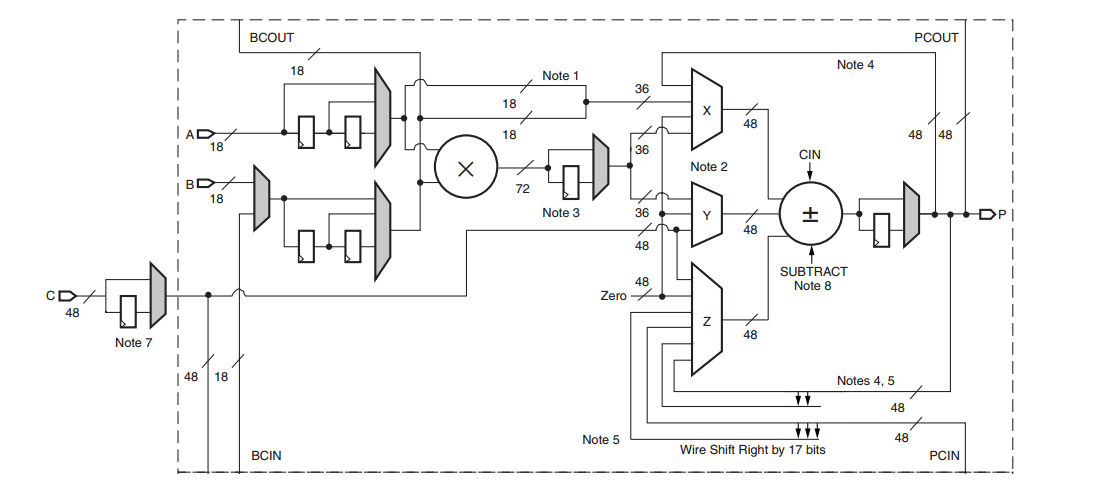
Figure 5. Block diagram of the DSP48 slices found in Virtex-4 devices. Image courtesy of Xilinx. Click to enlarge.
The equation for the output of the adder/subtractor is
$$Adder \ Out= \Big ( Z \pm (X+Y+C_{in}) \Big )$$
where X, Y, and Z denote the corresponding multiplexers’ output values. The multiplexers allow us to choose different inputs for the adder/subtractor. Multiplication is a typical application of the DSP slice. For example, we can configure a DSP48 slice to implement the following equation:
$$Adder \ Out = C \pm (A \times B + C_{in})$$
When the multiplier functionality is used, the X and Y multiplexer outputs must feed the adder, because the multiplier shown in the block diagram generates two partial results that are combined by the adder/subtractor to produce the final multiplication result. For more details, see page 21 of Xilinx's book, DSP: Designing for Optimal Results.
The registers in the path of the slice's different inputs allow us to have a pipelined design. For example, we can directly apply the input A to the math portion of the slice with no register in its path, or we can place one or two registers in its path. This is achieved by multiplexers (see Figure 5) that can choose inputs from before or after the registers.
The output of a DSP slice (labeled “P” in Figure 5) can be applied to the adder/subtractor of the same slice to implement an accumulator.
As Figure 5 suggests, a DSP slice supports several functions, including multiplication, multiplication followed by accumulation, fully pipelined multiplication, and circular barrel shifting. More advanced versions of the DSP48 slices incorporate some modifications, such as including a pre-adder block, which makes the slice even more versatile. For example, the pre-adder can be useful in implementing symmetric FIR filters (discussed above). Note that DSP slices are designed to efficiently implement the mentioned functions. That’s why a design based on DSP slices can achieve lower power consumption, higher performance, and more efficient silicon utilization compared to a design that uses the FPGA’s general-purpose fabric. For more details about the Xilinx DSP slices, please refer to the book mentioned above.
Implement Symmetric FIR Filters Using the DSP Slices
A simplified block diagram for the DSP slice of Figure 5 is shown in Figure 6 below.
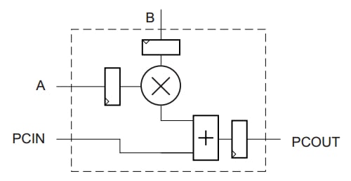
Figure 6
This simplified block diagram emphasizes that the output of one slice can be routed as an input to the adder/subtractor of the next slice. If we ignore the input registers shown in Figure 6, the schematic of Figure 6 is the same as the circuitry inside the dashed boxes of Figure 4. Hence, by cascading these DSP slices we can efficiently implement the FIR filter of Figure 4. In this case, we can implement the red adders (see Figure 4) using the general-purpose fabric slices of the FPGA.
Figure 7 shows an implementation of Figure 4 that uses the 7 Series DSP48 slices.

Figure 7. DSP48-based implementation of an eight-tap symmetric FIR filter. Image courtesy of Xilinx. Click to enlarge.
Here, the shaded adders implement the red adders of Figure 4, and the delay line can be implemented using the registers inside the slices. You can download the Xilinx VHDL code for the circuit of Figure 7 here (download will begin immediately if you click this link).
Conclusion
We derived a modular pipelined structure for symmetric FIR filters. We also looked at the structure of the Xilinx DSP slices, which can be used to implement several functions, including multiplication, multiplication followed by accumulation, fully pipelined multiplication, and circular barrel shifting. The 7 Series DSP48 slices are even more versatile and allow for a more efficient implementation of symmetric FIR filters.
To see a complete list of my articles, please visit this page.