 Facebook
 Google
 GitHub
 Linkedin
Designing a Self-Biasing Class C Amplifier
This article, part of AAC’s Analog Circuit Collection, explores a self-biased class C stage that could be used in an RF power amplifier.
This article, part of AAC’s Analog Circuit Collection, explores a self-biased class C stage that could be used in an RF power amplifier.
You are probably familiar with the distinction between an “ordinary” (i.e., low-power) amplifier circuit and a power amplifier. The low-power category includes most of the op-amp and in-amp circuits that are commonly found in analog and mixed-signal embedded systems; the goal is usually to apply significant voltage gain, or perhaps (in the case of a voltage follower) to reduce the source impedance. Power amplifiers, on the other hand, focus on increasing the signal’s current capacity so that it can provide more power to the load. Many low-voltage designs have no need for a power amplifier (PA), but PAs are standard components in RF systems: successful RF transmission requires sufficient power, and the PA delivers the high-power signal to the antenna.
Power amplifier topologies are grouped into categories called “classes.” In this article we’ll look at a Class C circuit. In the context of audio and general low-frequency power amplification, Class C amps are a bit exotic. They are common, however, in RF circuits, especially when battery life is a major concern. It’s important to understand that power amplifiers exhibit a fundamental trade-off between linearity and efficiency. Class A amps are highly linear, but they are biased in such a way as to increase current consumption. Class B amps are more efficient but less linear. Class C amps are even less linear than Class Bs, but they offer high efficiency. Thus, if you want a cell-phone battery to last as long as possible and you can somehow cope with an amplifier that produces a lot of distortion, Class C just might be the best choice.
You can find more information about Class C amps in AAC’s “Class C BJT Amplifiers” worksheet. In this article we’ll take a detailed look at a specific Class C implementation that is quite different from the circuit used in the worksheet. The implementation is based on a circuit given in the book RF Circuit Design, by Christopher Bowick. Full disclosure: This circuit is not exactly straightforward, and the book doesn’t provide an extensive explanation. As you read the article you’ll see that my mastery of the theory and design procedure is far from complete; if you have some relevant expertise and want to contribute to the discussion, the comments section (just scroll down to the bottom of the page) is ready and waiting.
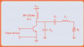
Here is the topology that we’ll be exploring:

Self-Bias
Amplifiers that are built around one or two transistors need to be biased—i.e., the DC conditions need to be arranged such that the transistor operates in a way that is conducive to amplification. Op-amps require biasing as well, but we don’t notice it because all the biasing work is done by the op-amp designer.
An interesting feature of Class C amplifiers is that they do not require an external bias circuit. The transistor is still biased, but it is biasing itself. The details here are a bit complicated and I don’t claim to understand them; instead I’ll quote from Bowick and hope that he has it right: if you want a transistor to become a Class C amp, you need to reverse bias the base-emitter junction; “if the base of the transistor is returned to ground through an RF choke, the base current flowing through the internal base-spreading resistance” can reverse bias the junction and thereby “force the transistor to provide its own bias.” One thing I will add is the following: The capacitor in series with the base (shown in the diagram above) appears to be merely a standard DC-blocking capacitor, but I believe that it also plays a role in maintaining the reverse bias. In other words, you would need the DC-blocking cap even if you knew that the input signal would never have a DC offset.
Not Even Half a Sine Wave
You may have already noticed something odd about the Class C circuit: there is no way that it can produce a sinusoidal output. Actually, it can’t even produce half of a sinusoid. The technical term here is “conduction angle.” A Class A circuit can generate an amplified version of the entire sine wave, and thus we say that it has a conduction angle of 360°. A Class B circuit conducts for only half of the cycle, so its conduction angle is 180°. The conduction angle of a Class C stage is significantly less than 180°.
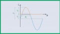
If you set up a Class C amp with nothing but a resistor between the BJT’s collector and the positive supply, you get an output waveform that looks like this:

No one would want to send this signal to an antenna. However—and this may be surprising if you’re thinking in the time domain instead of the frequency domain—the normal sine wave is somewhere inside that horribly distorted waveform. Let’s take a look at the FFT:

That spike at 100 MHz corresponds to the sinusoid that we want, which means that we need to do some serious filtering to suppress the harmonic content. We accomplish this by including an LC circuit between the collector and the positive supply. If we select the resonant frequency according to the system’s carrier frequency, you will be surprised at the quality of the sinusoid that we can produce from a Class C amp.
Design and Simulation
The standard Class C topology includes a parallel LC circuit that filters the transistor’s collector current. I cannot figure out why the Bowick version diverges from this model. He seems to be using a Pi filter composed of C3 (which in the book is labeled “bypass,” presumably because it is intended as a power-supply bypass capacitor), the primary winding of the output transformer, and C2. I used the equations found in this app note to calculate the values of L2 and C2.
Here is the simulation circuit:

Note the following:
- I used an LTspice ferrite bead component for the RF choke.
- The output transformer is created by adding two inductors and a “mutual inductance” statement.
- I used a fixed value for C2 because I’m working in the idealized SPICE world. In the original circuit, however, C2 is a variable capacitor, presumably because a real-world implementation would need to be adjusted in order to compensate for component tolerances and parasitic capacitance.
Here is the output signal:

I’d call that pretty good, considering what the unfiltered signal looks like.
I was wondering if I had found the optimal value for C2, so I used a “.step param” statement to test several different capacitances. The results are shown in the following plot; you can tell which trace is for which capacitance value because larger amplitude corresponds to smaller capacitance (i.e., orange is 10 pF, blue is 50 pF, ..., pink is 300 pF).

Both the 50 pF (blue) and the 92 pF (red) traces look good, and the next plot (which shows FFTs for the same group of waveforms) confirms that these two values exhibit good suppression of the second harmonic relative to the amplitude of the fundamental. Maybe the ideal value would be somewhere between 50 pF and 92 pF.

Conclusion
We discussed and examined a self-biasing Class C amplifier for RF circuits, and we looked at some interesting simulation results. If you want to continue the analysis on your own, you can download my LTspice schematic file by clicking on the orange button.


You wrote: “The standard Class C topology includes a parallel LC circuit that filters the transistor’s collector current. I cannot figure out why the Bowick version diverges from this model. He seems to be using a Pi filter composed of C3 (which in the book is labeled “bypass,” presumably because it is intended as a power-supply bypass capacitor), the primary winding of the output transformer, and C2.”
If you will examine the output tank (L2, C2) circuit closely, you will see that it is indeed parallel resonant, with link (L3) couppling to the load (R2). The “Bypass” (C3) has a reactance at the signal frequency (100 MHz) which is negligibly small compared to that of L2 and C2. The AC equivalent circuit then becomes L2 in parallel with C2, and one end of this parallel combination is grounded, and the other end is connected to Q1’s collector. The value of C2 will be very close to optimum when the magnitude of C2’s reactance plus strays equals that of L2 at the signal frequency - in other words, resonant at the signal frequency.
Thank you. How to calculate the efficiency? I can see that the input signal is 1.5Vpp- 0.7App. and the output is 4Vpp 0.06App! how is the power been amplified ?