Facebook
 Google
 GitHub
 Linkedin
Explore Negative Voltage Using LTspice and a Negative Voltage Generator
In this article, we’ll use SPICE simulations to explore the theory and behavior of negative voltages.
In a previous article, I provided a primarily theoretical explanation of negative voltage. I would like to continue this topic with demonstrations of negative voltage in action combined with explanations that will help to strengthen our understanding of negative voltage. To do this, we’ll use LTspice for the “hands-on” work here, but if you have access to test equipment and some common electronic components, you can fairly easily re-create the first simulation as a physical circuit measured with an oscilloscope.
The Capacitor: A Negative Voltage Generator
First, let’s start with one of the simplest negative voltage-generating circuits that I can think of, which consists of a pulsed voltage source, a capacitor, and a resistor. This circuit can be seen in Figure 1 below.
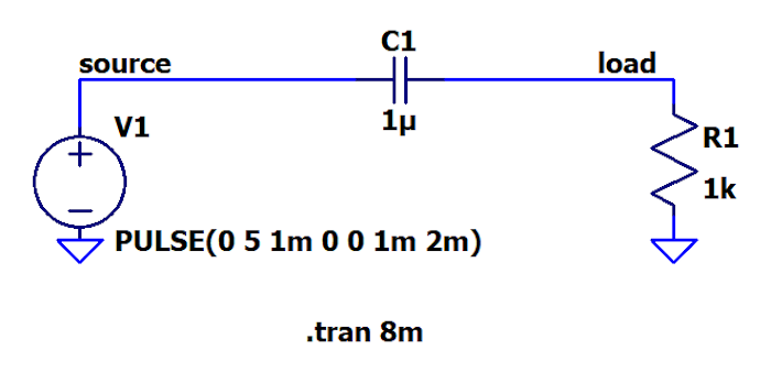
Figure 1. An example negative voltage-generating circuit with a pulsed voltage source, a capacitor, and a resistor.
A transient simulation of this circuit produces a waveform (Figure 2) with a familiar pattern; if you’ve spent some time experimenting with circuitry in an electronics lab, you’ve probably seen something similar.
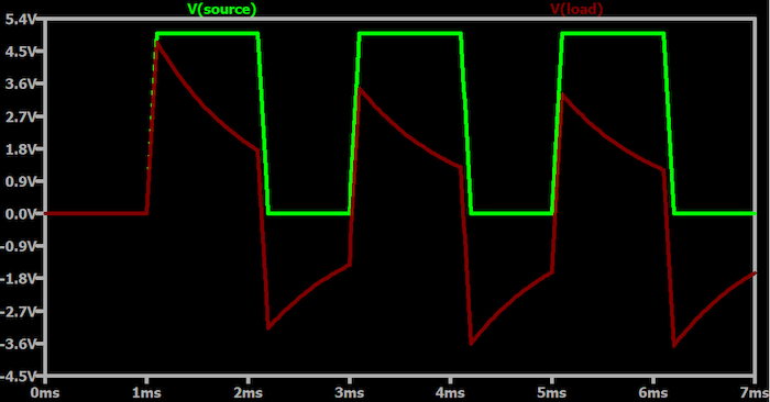
Figure 2. An example waveform from Figure 1's transient simulation.
Clearly, we have generated negative voltages. I wouldn’t call this a negative voltage power supply since this circuit can’t produce a stable negative voltage for powering other components; however, this simulation shows that negative voltages are not exotic phenomena produced only by complex circuitry.
With that in mind, what exactly is happening here? Let’s take a look.
When the source voltage transitions from 0 V to 5 V, the left side of the capacitor also transitions to 5 V; the positive source terminal and the left-hand terminal of the capacitor are actually the same nodes, so they must have the exact same voltage. The voltage of the right-hand terminal of the capacitor labeled V(load) in the plot tracks the rising edge of the source voltage because the capacitor is almost “transparent” to rapidly changing voltages. Note that, as explained in the All About Circuits textbook, the current through a capacitor is directly proportional to the rate of change of voltage.
When the source voltage stabilizes at 5 V, the capacitor is charged. The capacitor now functions like an open circuit, meaning that it blocks current that otherwise would be supplied by the source voltage, and it begins to discharge through the resistor. The capacitor is partially discharged when the source voltage transitions back to 0 V, and this is where things get interesting.
The source voltage jumps from 5 V to 0 V, but the voltage across a capacitor cannot change instantaneously—a capacitor needs time to release its stored charge. Since the left-hand terminal of the capacitor has the same voltage as the positive terminal of the source, the right-hand terminal of the capacitor must quickly decrease by 5 V so that the voltage across the capacitor stays the same. If the right-hand terminal of the capacitor is at 1.5 V and must decrease by 5 V, there’s only one place to go: into the negative voltage territory.
As I explained in the aforementioned previous article, positive and negative voltages both provide energy for current flow, but with negative voltages, current flows from the zero-volt reference node into the negative voltage node. We can see this behavior (Figure 3) in the simulation if we add a current trace to the plot.
Figure 3. Plot showing the simulation with an added current trace.
In Figure 3, notice how the current is negative when the load voltage is negative. A negative current doesn’t mean that there is a “less than zero” movement of charge through the conductors. It simply means that the direction of the current flow is opposite to the reference direction. In this simulation, the current flowing down through the resistor is defined as positive current, and since a negative V(load) causes current to flow from the ground node and then upward through the resistor, LTspice identifies the current as negative.
Capacitors and Switches: A Negative Voltage Power Supply
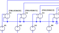
With the help of some voltage-controlled switches and an additional capacitor, we can convert a capacitor into a negative voltage generator that produces a stable voltage and supplies power to other components. Consider the circuit shown below in Figure 4; this is an LTspice version of a switched-capacitor inverter.
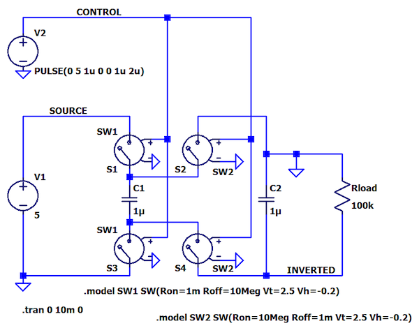
Figure 4. An LTspice version of a switched-capacitor inverter diagram.
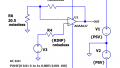
Figure 5 shows an example of a more simplified schematic diagram.
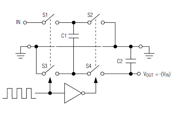
Figure 5. An example of a simplified schematic diagram of an IC using a switched-capacitor topology to generate an inverted supply voltage. Image used courtesy of Analog Devices
The basic idea is that we charge a capacitor (C1) to an input voltage (VIN), disconnect the charged capacitor from the input source, and then connect the charged capacitor to a second capacitor (C2) such that the higher-voltage terminal of C1 is paired with the grounded terminal of C2. This switching technique forces the voltage of C2’s other terminal to decrease by VIN volts relative to the ground. Thus, the output voltage shifts into the negative voltage territory.
Perhaps you can see why this type of circuit is also called a charge pump. We’re pumping charge from an input supply to one capacitor and then to a second capacitor whose terminals are connected in such a way as to invert the voltage. The pumping action is governed by the square waves that control the switches.
The digital inverter, shown in the simplified schematic, ensures that S1 and S3 are on while S2 and S4 are off, and vice versa. In my LTspice circuit, the two voltage-controlled switches are controlled by the same square wave. I impose the proper on/off relationship simply by defining two different SW models:
- SW1 has low resistance for the "on" state and high resistance for the "off" state
- SW2 has high resistance for the “on” state and low resistance for the “off” state
Below is a plot of the output voltage labeled INVERTED in the LTspice schematic.
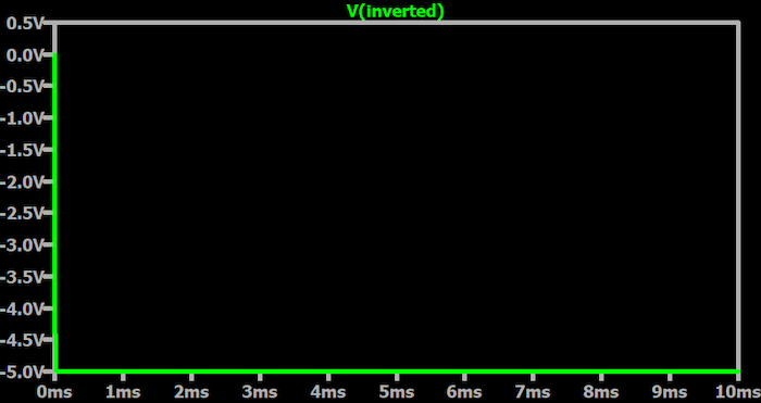
Figure 6. The plot of the output voltage, which is labeled as INVERTED in the LTspice schematic.
If we zoom in, we can see in Figure 7 that the circuit needs a bit of time to pump its way down to negative VIN.
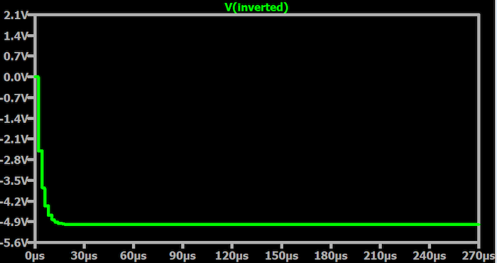
Figure 7. A zoomed-in version of the circuit's simulated plot.
Using LTspice to Understand Negative Voltage
I hope that these simulations have helped you to understand a bit more about what negative voltage is and how ordinary components can cause voltages to shift below “ground,” i.e., below the circuit’s reference voltage. I plan to further explore the design and performance of the LTspice switched-capacitor inverter in a future article.