 Facebook
 Google
 GitHub
 Linkedin
How to Design a Custom PCB Holder: Mechanical Considerations for a High-Precision Sensor System
When working with high-precision sensors, it's crucial to consider housing. In this article, we discuss an approach to designing a custom board holder for an inclinometer subsystem.
When working with high-precision sensors, it's crucial to consider housing. In this article, we discuss the mechanical design considerations at play in a custom board design for an inclinometer subsystem.
There are many considerations for mechanical design when you're designing a system with a high level of precision. I recently designed an inclinometer-based custom PCB with so much precision that I need to design a heavy, stable housing to protect the integrity of the data it gathers.
As I mentioned in my inclinometer subsystem overview, the overall project should allow a resolution of 0.001°, meaning that the sensor will pick it up if the board is moved by even 1 µm. This means that you'd need to digitally recalibrate the board every time it's adjusted in its holder. To make things easier, I decided to fix my board to a holder for less need for constant digital recalibration.

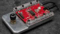
Shown above is the assembled board held in the aluminum test fixture during preliminary testing.
Please check out the links below to learn more about the precision inclinometer project series. This article refers specifically to the PCB layout article.
- How to Design a Precise Inclinometer on a Custom PCB (full project overview)
- Schematic Design
- PCB Layout
- Firmware Design
Manual Board Adjustment with Differential-Drive Screws
Because I am Mark "Hard-way" Hughes, I decided to add a manual adjustment system. On one end of the holder, I chose a differential-drive screw mechanism. On the other, I added two additional M3 polished acorn nuts at the opposite end of the board holder. These two non-adjustable feet are screwed to the underside of the board and become a pivot point opposite the differential screw. Additionally, this arrangement allows some amount of adjustment for testing the project.

An exploded render of the PCB holder, alignment pins, PCB, and PCB clamps
Differential-screw mechanisms have two threads of slightly-different pitch that simultaneously rotate around a central axis. They are arranged so that as one screw advances, the other retreats. The result is a compound screw whose effective pitch is the difference of the pitch of the original two screws.
This video demonstrates a generic differential screw while this video shows the Thorlabs differential screw used in this project.

A render of the differential screw. Thread size has been exaggerated in this illustration. Image by Mark Hughes
This differential screw mechanism can be adjusted in multiple ways. Rotating the coarse part (shown in blue above) provides rough adjustment. Rotating the fine part (shown in red above) provides fine adjustment. Rotating the middle part (shown in green above) simultaneously affects both the rough and fine, providing microfine (differential) adjustment.
Bespoke differential screw mechanisms can be manufactured by your friendly neighborhood machinist if you have access to the company credit card. Due to budgetary concerns, I settled on a 25 µm/rev differential adjustment screw manufactured by Thorlabs.
One full revolution of the mechanism changes the height of the end of the PCB holder by 25µm, but the screw can be turned in smaller amounts.
In the case of this differential screw, 1 µm corresponds to a rotation of approximately 15°. While this is not an ideal level of adjustment, it is at least within the realm of plausibility. And, as a backup, I have the ability to calibrate the device digitally.
PCB Mechanical Design: Mitigating Heat and Mechanical Stress
We incorporated some mechanical design considerations into our PCB design, itself.
Six 3mm notches are placed 1-inch on center along the long edges of the board that will mate with indexing pins in the aluminum carrier. The PCB is held in place by two 3” long aluminum clamping pieces that will be loosely held against the PCB with M3x0.5 or #4-40 hardware.
Rather than using fixed mounting holes that create concentrated stress points, this design allows a small amount of pressure to be applied over a large area of the board, securing it while simultaneously allowing some movement parallel to the plane of the board.

4-layer PCB stack-up shown above. Dark green is the ground net. Red is the 12V net. Salmon is the 3V3 net. Light green is the 2V5 net. Dark blue is the 5V0 VRef net.
The only component of this board with mechanical considerations specified in the datasheet is the 5V Voltage reference U4, Linear’s LT1027LS8.
The datasheet indicates that “power and ground planes should be omitted under the voltage reference IC,” which is relatively easy to accomplish with route keepouts. Of more immediate concern is the directive to “[cut slots] through the PC board on all four sides. The slots should be as long as possible, and the corners just large enough to accommodate routing of traces.”

Figure 8 from datasheet that shows suggest board cut-out patterns to use.
This is done to minimize any mechanical stresses on the PCB near the voltage reference. Changes in humidity, as well as temperature, can cause the PCB to shrink or stretch, which can, in turn, apply stress to the LT1027LS8 package. These proposed cutouts reduce any thermal conduction of heat from nearby components, as well as provide mechanical stress relief.
The width of the cut, sometimes called the “kerf,” is determined by the PCB manufacturer’s capabilities—which, in my case, is a lower limit of 1 mm. I chose to extend each cut with a small angled relief to extend the slot and further insulate the components.
It might be possible to further mitigate stress with more elaborate designs. If you have any advice on this, please let me know in the comments below, as I did not consult with a mechanical engineer for this design.
Cutting power and ground planes can be a dangerous thing to do during PCB layout. All signals will find a return route and an interrupted ground plane can make that path unpredictable.
And, in keeping with the “Hard-way Hughes” paradigm, I should take this opportunity to note that the sensor provides ratiometric output and both the ADC reference input and the sensor power input are fed by the output of this voltage reference. Ratiometric means that the output scales linearly with the reference voltage, so a change in the reference level should affect the input and output equally.
So the voltage reference could drift substantially before it began to affect the data conversion, so it is possible that the extra work required to incorporate the recommendations for the datasheet are largely unnecessary for this design.
I do regret not incorporating a voltage-follower/buffer between the voltage reference and the ADC, especially since I had one on the board with two available channels. I’ll have to test the board to determine whether or not the design performs acceptably without it.

An artistic impression of the thermal/stress finite-element analysis
The above artistic impression of a mixed thermal/stress finite-element analysis illustrates how the board cutouts serve to mechanically and thermally isolate the interior section of the board from the heat generated by the ICs, as well as some theoretical pressures applied to the exterior sides of the board. The board cutouts reduce the overall stresses applied to the area of the board occupied by the voltage reference IC.
There are no calibration switches on the PCB, itself, because pressing them might disturb the alignment of the board. Instead, a 20-pin 0.5” FFC takes multiple capacitive-touch lines from the microcontroller to an exterior control panel that is not yet designed. Data will be taken from the board via the USB to UART interface.
Summary
When creating high-precision analog circuits, some devices require significant consideration for maximum performance. While I might have easily ignored best-practices or omitted some of the manufacturer recommendations in this design, I made every attempt to integrate them for educational purposes.


Very interesting article, learned about differential screw and other considerations. Thanks.