Facebook
 Google
 GitHub
 Linkedin
How to Interface the Mojo V3 FPGA Board with a 16x2 LCD Module: Block Diagram and Verilog Code
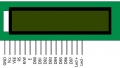
This article will discuss the details of interfacing a basic 16x2 LCD module with an FPGA.
This article will discuss the details of interfacing a basic 16x2 LCD module with an FPGA.
In the previous article, we examined the building blocks needed for interfacing an FPGA with a common 16x2 LCD module. We saw that the main building blocks are ROM, some DFFs, and multiplexers. Additionally, we needed an FSM (finite state machine) to control these building blocks. In this article, we’ll look at the details of designing the FSM. Then, we’ll write the Verilog code for the different blocks and use the Mojo V3 board to verify our design.
The System Block Diagram
The FPGA-LCD interface block diagram is shown in Figure 1 below:
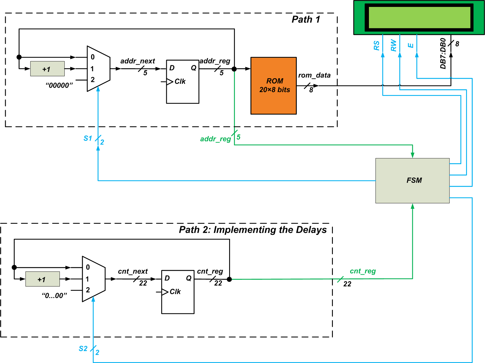
Figure 1
As you can see, the FSM has two inputs (addr_reg and cnt_reg) and five outputs (s1, s2, RS, RW, and E). The FSM inputs allow us to monitor the status of the “Path 1” and “Path 2” blocks.
The “s1” output controls “Path 1” and, consequently, the data applied to the DB7-DB0 pins. The “s2” output controls the “Path 2” block and can be used to generate the required time delays. The “RS”, “RW”, and “E” outputs generate the appropriate waveforms for the LCD control pins.
Designing the FSM
An initial design for the FSM is shown in Figure 2. The FSM has three states: “idle”, “lcd_init”, and “lcd_print”.
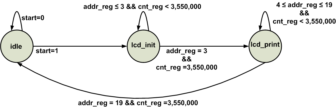
Figure 2
The “idle” State
During the “idle” state, the outputs are initialized. The ASM (Algorithmic State Machine) block for this state is shown in Figure 3.
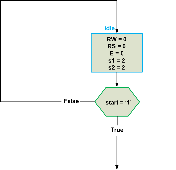
Figure 3
When in the “idle” state, the outputs “RW”, “RS”, and “E” are initialized to logic low. The “s1” and “s2” outputs are equal to 2 so that the DFFs of “Path 1” and “Path 2” are reset at the next clock edge (see Figure 1). Note the additional input (“start”) for the FSM. This will be connected to a pushbutton on the breadboard. Setting the “start” input to logic high will start the process of printing on the LCD.
The “lcd_init” State
In this state, the LCD module is initialized. To this end, the four commands (0x38, 0x06, 0x0C, and 0x01) that are stored at addresses 0 to 3 of the ROM should be applied to the LCD data pins. That’s why the state diagram of Figure 2 incorporates the term addr_reg = 3 as a condition for transitioning from “lcd_init” to the next state (“lcd_print”).
The other term for the state transition condition is cnt_reg = 3,550,000. Each byte of the ROM should be applied to the LCD data pins for a sufficient amount of time (71 ms in our design). The condition cnt_reg = 3,550,000 makes sure that the LCD had enough time (71 ms) to read the data pins. Therefore, the condition addr_reg = 3 && cnt_reg = 3,550,000 means that the fourth command stored in the ROM is applied to the LCD for about 71 ms. When this condition is satisfied, the LCD is initialized successfully and we can put the message data on DB7-DB0.
The ASM block for the “lcd_init” state is shown in Figure 4.
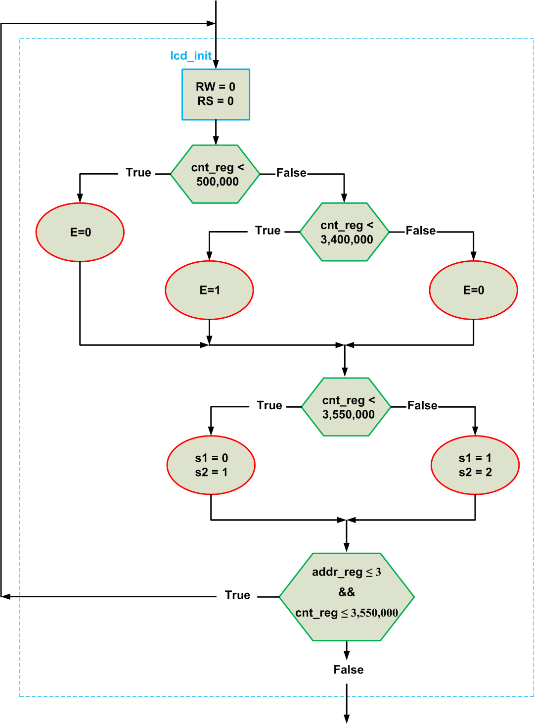
Figure 4
Before examining the above ASM block, let’s see how the threshold numbers for cnt_reg are determined. The timing diagram for a write operation of the LCD module is shown in Figure 5.
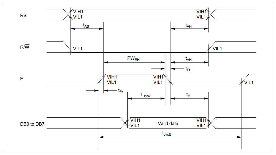
Figure 5. Image used courtesy of HITACHI.
Note that the “E” signal should go to logic high after tAS. It remains at logic high for PWEH and then transitions to logic low tH before the next write operation. In this article, tAS, PWEH, and tH are 10 ms, 58 ms, and 3 ms, respectively. The waveform for the “E” signal is as shown in Figure 6.
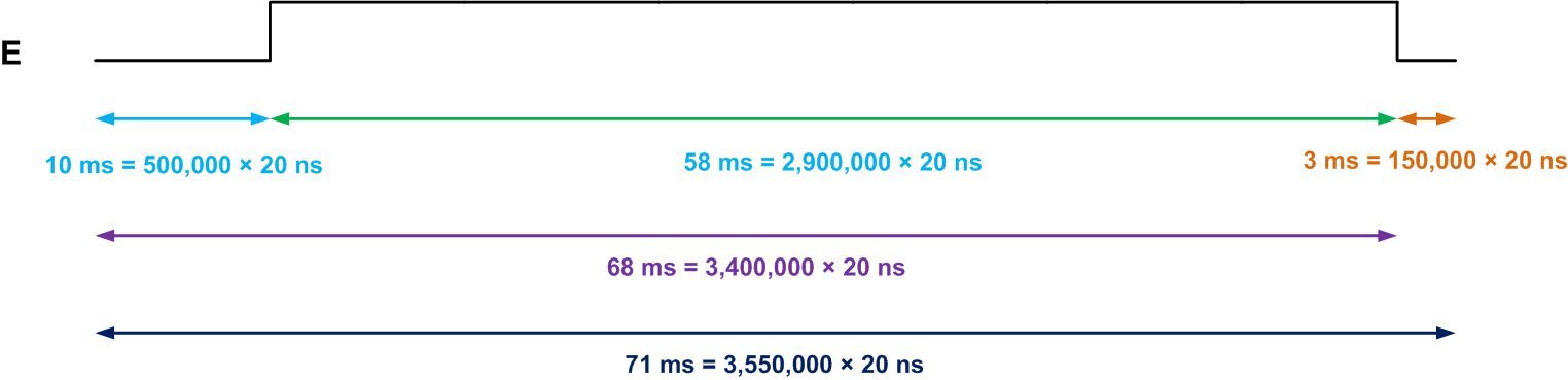
Figure 6
The figure also shows the equivalent number of counts for each time delay. Note that the clock frequency of the Mojo V3 board is 50 MHz (clock period = 20 ns). As shown in Figure 4, we check the value of “cnt_reg” to set an appropriate value for E. For example, when the “cnt_reg” signal is greater than 500,000 and less than 3,400,000, the E signal should be logic high.
Again, the “s1” and “s2” outputs are determined based on the value of the “cnt_reg” signal. If “cnt_reg” is less than 3,550,000 (equivalent to 71 ms), we have not reached the end of the current write operation (see Figure 6). Therefore, the data applied to the LCD should not change (s1 = 0) and the counter should count (s2 = 1). However, when “cnt_reg” is greater than 3,550,000 (equivalent to 71 ms), we have reached the end of the current write operation. In this case, the data in the next address of the ROM should be applied to the LCD (s1 = 1) and the counter should be reset to 0 (s2 = 2) (see Figure 1).
As discussed before, we have four LCD configuration commands stored at addresses 0 to 3 of the ROM. When the fourth command (addr_reg = 3) is applied to the LCD for 71 ms (cnt_reg = 3,550,000), we should go to the “lcd_print” state that sends the message data to the LCD. This is achieved by the last hexagon in the ASM block.
Note that the “RS” input of the LCD module specifies whether DB7-DB0 should be treated as an instruction code (RS=0) or as data (RS=1). Hence, during the “lcd_init” state, the RS pin should be at logic low. The RW pin specifies whether we are writing to the module (RW=0) or reading from it (RW=1). In both the “lcd_init” and “lcd_print” states, we are performing a write operation and RW should be logic low.
The “lcd_print” State
The “lcd_print” state is quite similar to the “lcd_init” state except that RS should be logic high (because now DB7-DB0 should be treated as data rather than an instruction code). Besides, the threshold values checked for the addr_reg signal should change because the message is stored at addresses 4 to 19 of the ROM. With these modifications, we get the ASM block shown in Figure 7.
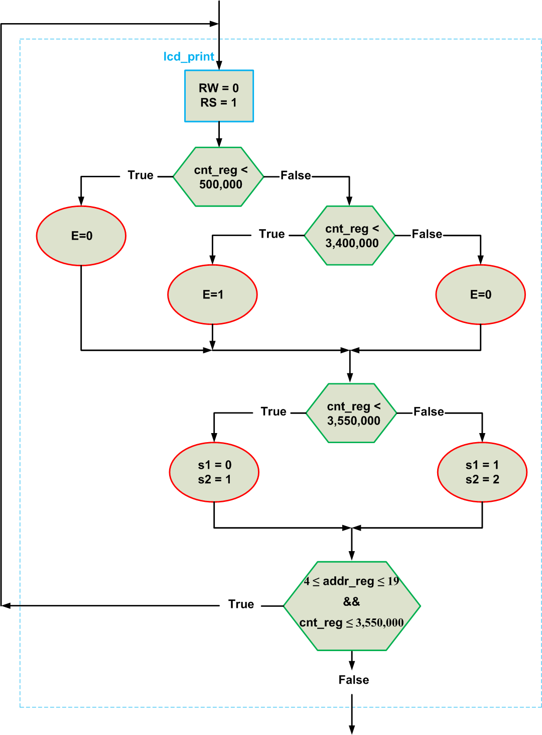
Figure 7
Finally, connecting all these ASM blocks together, we obtain the ASM chart shown in Figure 8.

Figure 8 Click to enlarge.
The Verilog Code
If we have the block diagram of Figure 1 and the above ASM chart, it’s an easy task to create the Verilog description of the system. Let’s take a look at the code of the different building blocks:
Path 1
For the “path 1” block, we need a 20✕8 ROM:
//Path 1: ROM
wire [7:0] rom_data [19:0];

assign rom_data[0] = 8'h38;
assign rom_data[1] = 8'h06;
assign rom_data[2] = 8'h0C;
assign rom_data[3] = 8'h01;

assign rom_data[4] = " ";
assign rom_data[5] = " ";
assign rom_data[6] = "H";
assign rom_data[7] = "E";
assign rom_data[8] = "L";
assign rom_data[9] = "L";
assign rom_data[10] = "O";
assign rom_data[11] = " ";
assign rom_data[12] = "W";
assign rom_data[13] = "O";
assign rom_data[14] = "R";
assign rom_data[15] = "L";
assign rom_data[16] = "D";
assign rom_data[17] = "!";
assign rom_data[18] = " ";
assign rom_data[19] = " ";

assign data = rom_data[addr_reg];
This specifies that “rom_data” is a 2D array of type wire. Note that, in Verilog, the second dimension of the array comes after the name of the array. The desired values are assigned to the array and, finally, the output of the ROM is assigned to “data”; “data” is the output of our design and will be connected to DB7-DB0 of the LCD module.
The registers and the multiplexer of “Path 1” can be described by the following code:
reg [4:0] addr_reg, addr_next;

//Path 1: Registers
always@(posedge clk, posedge rst)
begin
	if(rst)
		addr_reg <= 5'b0;
	else
		addr_reg <= addr_next;
end

//Path 1: Mux
always @*
	case(s1)
		2'b00:
			addr_next = addr_reg;

		2'b01:
			addr_next = addr_reg + 1'b1;

		2'b10:
			addr_next = 5'b0;

		default:
			addr_next = addr_reg;
	endcase
Path 2
The “Path 2” block is described as follows:
reg [21:0] cnt_reg, cnt_next;

//Path 2: Registers
always@(posedge clk, posedge rst)
begin
	if(rst)
		cnt_reg <= 21'h0;
	else
		cnt_reg <= cnt_next;
end

//Path 2: Mux
always @*
	case(s2)
		2'b00:
			cnt_next = cnt_reg;

		2'b01:
			cnt_next = cnt_reg + 1'b1;

		2'b10:
			cnt_next = 21'h0;

		default:
			cnt_next = cnt_reg;
	endcase
The FSM
To describe an FSM in Verilog HDL, we can use the “localparam” statement to define symbolic constants that represent the FSM’s states. Our FSM has three states. These state can be described by the following “localparam”:
localparam [1:0]	idle      = 2'b00,
			lcd_init  = 2'b01,
			lcd_print = 2'b10;
To store the system state, we define a two-bit register:
reg [1:0] state_reg, state_next;

//State Registers
always@(posedge clk, posedge rst)
begin
	if(rst)
		state_reg <= idle;
	else
		state_reg <= state_next;
end
Then, we should describe the combinational circuit that determines the next state of the FSM. This part of the code can be written based on the hexagons of the ASM chart in Figure 8. Though, note that the following code has simplified the state transition conditions that we derived before.
//Next State Logic
always @*
begin
	case(state_reg)
		idle:
			if(start)
				state_next = lcd_init;
			else
				state_next = idle;

		lcd_init:
			if(addr_reg == 5'h03 && cnt_reg == 3550000)
				state_next = lcd_print;
			else
				state_next = lcd_init;

		lcd_print:
			if(addr_reg == 5'h19 && cnt_reg == 3550000)
				state_next = idle;
			else
				state_next = lcd_print;

		 default:
				state_next = idle;
		endcase
end
Finally, we should write the Verilog code for the FSM outputs. This part of the code can be written based on the ellipses of Figure 8, which represent conditional assignments of the FSM.
//Output Logic
always @*
begin
		case(state_reg)
			idle:
				begin
				s1 = 2'b10;
				s2 = 2'b10;
				RW = 0;
				RS = 0;
				E = 0;
				end

			lcd_init:
				begin
				s1 = 2'b00;
				s2 = 2'b01;
				RS = 0;
				RW = 0;
				E = 0;
				if (cnt_reg >= 500000)
					E = 1;
				if (cnt_reg >= 3400000)
					E = 0;
				if (cnt_reg == 3550000)
				begin
					s1 = 2'b01;
					s2 = 2'b10;
				end
				end

			lcd_print:
				begin
				s1 = 2'b00;
				s2 = 2'b01;
				RS = 1;
				RW = 0;
				E = 0;
				if (cnt_reg >= 500000)
					E = 1;
				if (cnt_reg >= 3400000)
					E = 0;
				if (cnt_reg == 3550000)
				begin
					s1 = 2'b01;
					s2 = 2'b10;
				end
				end
			default:
				begin
				s1 = 2'b10;
				s2 = 2'b10;
				RW = 0;
				RS = 0;
				E = 0;
				end

		endcase
end
The Mojo Project
Now, you can grab a copy of the Mojo Base Project and add the above code segments to it. Remember that you’ll have to modify the inputs and outputs of the top-level Verilog module.
If you’re not already familiar with operating the Mojo, visit this page for some great Verilog-based tutorials.
The final code will be:
module mojo_top(
    // 50MHz clock input
    input clk,
    // Input from reset button (active low)
    input rst_n,
    // cclk input from AVR, high when AVR is ready
    input cclk,
    // Outputs to the 8 onboard LEDs
    output[7:0]led,
    // AVR SPI connections
    output spi_miso,
    input spi_ss,
    input spi_mosi,
    input spi_sck,
    // AVR ADC channel select
    output [3:0] spi_channel,
    // Serial connections
    input avr_tx, // AVR Tx => FPGA Rx
    output avr_rx, // AVR Rx => FPGA Tx
    input avr_rx_busy, // AVR Rx buffer full

	 //My Inputs and Outputs
	 input start,
	 output [7:0] data,
	 output reg RS, RW, E
	 );

wire rst = ~rst_n; // make reset active high

// these signals should be high-z when not used
assign spi_miso = 1'bz;
assign avr_rx = 1'bz;
assign spi_channel = 4'bzzzz;

assign led[7:0] = 5'h00;

localparam [1:0] idle      = 2'b00,
					  lcd_init  = 2'b01,
					  lcd_print = 2'b10;

reg [1:0] state_reg, state_next;
reg [4:0] addr_reg, addr_next;
reg [21:0] cnt_reg, cnt_next;
reg [1:0] s1, s2;

//State Registers
always@(posedge clk, posedge rst)
begin
	if(rst)
		state_reg <= idle;
	else
		state_reg <= state_next;
end


//Next State Logic
always @*
begin
	case(state_reg)
		idle:
			if(start)
				state_next = lcd_init;
			else
				state_next = idle;

		lcd_init:
			if(addr_reg == 5'h03 && cnt_reg == 3550000)
				state_next = lcd_print;
			else
				state_next = lcd_init;

		lcd_print:
			if(addr_reg == 5'h19 && cnt_reg == 3550000)
				state_next = idle;
			else
				state_next = lcd_print;

		 default:
				state_next = idle;
		endcase
end

//Output Logic
always @*
begin
		case(state_reg)
			idle:
				begin
				s1 = 2'b10;
				s2 = 2'b10;
				RW = 0;
				RS = 0;
				E = 0;
				end

			lcd_init:
				begin
				s1 = 2'b00;
				s2 = 2'b01;
				RS = 0;
				RW = 0;
				E = 0;
				if (cnt_reg >= 500000)
					E = 1;
				if (cnt_reg >= 3400000)
					E = 0;
				if (cnt_reg == 3550000)
				begin
					s1 = 2'b01;
					s2 = 2'b10;
				end
				end

			lcd_print:
				begin
				s1 = 2'b00;
				s2 = 2'b01;
				RS = 1;
				RW = 0;
				E = 0;
				if (cnt_reg >= 500000)
					E = 1;
				if (cnt_reg >= 3400000)
					E = 0;
				if (cnt_reg == 3550000)
				begin
					s1 = 2'b01;
					s2 = 2'b10;
				end
				end
			default:
				begin
				s1 = 2'b10;
				s2 = 2'b10;
				RW = 0;
				RS = 0;
				E = 0;
				end

		endcase
end

//Path 1: ROM
wire [7:0] rom_data [19:0];

  assign rom_data[0] = 8'h38;
  assign rom_data[1] = 8'h06;
  assign rom_data[2] = 8'h0C;
  assign rom_data[3] = 8'h01;

  assign rom_data[4] = " ";
  assign rom_data[5] = " ";
  assign rom_data[6] = "H";
  assign rom_data[7] = "E";
  assign rom_data[8] = "L";
  assign rom_data[9] = "L";
  assign rom_data[10] = "O";
  assign rom_data[11] = " ";
  assign rom_data[12] = "W";
  assign rom_data[13] = "O";
  assign rom_data[14] = "R";
  assign rom_data[15] = "L";
  assign rom_data[16] = "D";
  assign rom_data[17] = "!";
  assign rom_data[18] = " ";
  assign rom_data[19] = " ";

  assign data = rom_data[addr_reg];

//Path 1: Registers
always@(posedge clk, posedge rst)
begin
	if(rst)
		addr_reg <= 5'b0;
	else
		addr_reg <= addr_next;
end

//Path 1: Mux
always @*
	case(s1)
		2'b00:
			addr_next = addr_reg;

		2'b01:
			addr_next = addr_reg + 1'b1;

		2'b10:
			addr_next = 5'b0;

		default:
			addr_next = addr_reg;
	endcase


//Path 2: Registers
always@(posedge clk, posedge rst)
begin
	if(rst)
		cnt_reg <= 21'h0;
	else
		cnt_reg <= cnt_next;
end

//Path 2: Mux
always @*
	case(s2)
		2'b00:
			cnt_next = cnt_reg;

		2'b01:
			cnt_next = cnt_reg + 1'b1;

		2'b10:
			cnt_next = 21'h0;

		default:
			cnt_next = cnt_reg;
	endcase

endmodule
Schematic and the UCF File
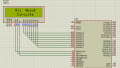
Figure 9 below shows the connections between the Mojo and the LCD module.
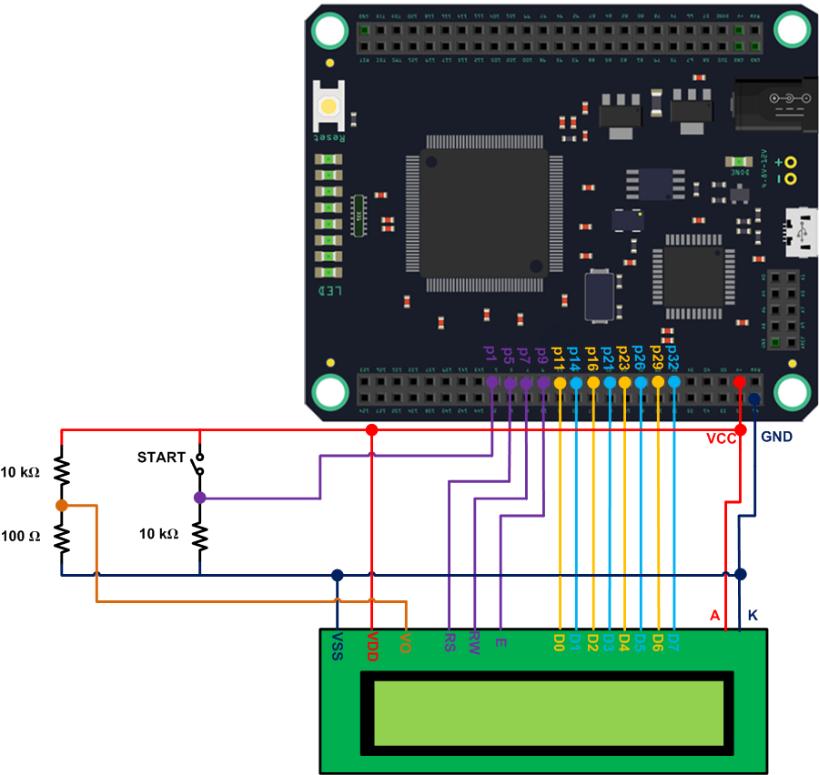
Figure 9
Now, we can add some new constraints to the User-defined Constraint File (UCF) of the Mojo Base Project to specify the FPGA pins that are connected to the inputs/outputs of our top-level module. The first several lines in the following UCF file are already included in the Mojo Base Project; however, the last 12 lines specify FPGA pins connected to the DB7-DB0, start, RS, RW, and E signals in our code.
#Created by Constraints Editor (xc6slx9-tqg144-3) - 2012/11/05
NET "clk" TNM_NET = clk;
TIMESPEC TS_clk = PERIOD "clk" 50 MHz HIGH 50%;

# PlanAhead Generated physical constraints
NET "clk" LOC = P56 | IOSTANDARD = LVTTL;
NET "rst_n" LOC = P38 | IOSTANDARD = LVTTL;

NET "cclk" LOC = P70 | IOSTANDARD = LVTTL;

NET "led<0>" LOC = P134 | IOSTANDARD = LVTTL;
NET "led<1>" LOC = P133 | IOSTANDARD = LVTTL;
NET "led<2>" LOC = P132 | IOSTANDARD = LVTTL;
NET "led<3>" LOC = P131 | IOSTANDARD = LVTTL;
NET "led<4>" LOC = P127 | IOSTANDARD = LVTTL;
NET "led<5>" LOC = P126 | IOSTANDARD = LVTTL;
NET "led<6>" LOC = P124 | IOSTANDARD = LVTTL;
NET "led<7>" LOC = P123 | IOSTANDARD = LVTTL;

NET "spi_mosi" LOC = P44 | IOSTANDARD = LVTTL;
NET "spi_miso" LOC = P45 | IOSTANDARD = LVTTL;
NET "spi_ss" LOC = P48 | IOSTANDARD = LVTTL;
NET "spi_sck" LOC = P43 | IOSTANDARD = LVTTL;
NET "spi_channel<0>" LOC = P46 | IOSTANDARD = LVTTL;
NET "spi_channel<1>" LOC = P61 | IOSTANDARD = LVTTL;
NET "spi_channel<2>" LOC = P62 | IOSTANDARD = LVTTL;
NET "spi_channel<3>" LOC = P65 | IOSTANDARD = LVTTL;

NET "avr_tx" LOC = P55 | IOSTANDARD = LVTTL;
NET "avr_rx" LOC = P59 | IOSTANDARD = LVTTL;
NET "avr_rx_busy" LOC = P39 | IOSTANDARD = LVTTL;

#My Constraints
NET "start" LOC = P1 | IOSTANDARD = LVTTL;
NET "RS" LOC = P5 | IOSTANDARD = LVTTL;
NET "RW" LOC = P7 | IOSTANDARD = LVTTL;
NET "E" LOC = P9 | IOSTANDARD = LVTTL;
NET "data<0>" LOC = P11 | IOSTANDARD = LVTTL;
NET "data<1>" LOC = P14 | IOSTANDARD = LVTTL;
NET "data<2>" LOC = P16 | IOSTANDARD = LVTTL;
NET "data<3>" LOC = P21 | IOSTANDARD = LVTTL;
NET "data<4>" LOC = P23 | IOSTANDARD = LVTTL;
NET "data<5>" LOC = P26 | IOSTANDARD = LVTTL;
NET "data<6>" LOC = P29 | IOSTANDARD = LVTTL;
NET "data<7>" LOC = P32 | IOSTANDARD = LVTTL;
Conclusion
With FPGAs, we usually have to look at the problem at the lowest level of the design. What we have are logic gates and some basic building blocks such as adders and comparators. Although this can make FPGA design somewhat difficult, FPGAs do offer several advantages.
In this project, we examined building blocks used to interface an FPGA with a common 16x2 LCD module. A ROM, some DFFs, and multiplexers are required to implement the FPGA-to-LCD interface. Additionally, we need an FSM to control these building blocks. We looked at the details of designing the FSM and found the Verilog description for the different building blocks of the design. Finally, we downloaded our code to the Mojo V3 board and displayed the “HELLO WORLD!” message on the LCD.
To see a complete list of my articles, please visit this page.