Facebook
 Google
 GitHub
 Linkedin
How to Interface the Mojo v3 FPGA Board with a 16x2 LCD Module
This article will discuss the details of interfacing a basic 16x2 LCD module with an FPGA.
This article will discuss the details of interfacing a basic 16x2 LCD module with an FPGA.
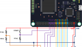
In this tutorial, we’ll use the Verilog HDL to design a digital circuit that interfaces with the common LCD modules that are based on the HD44780 LCD controller/driver chip. The Mojo V3 FPGA board will be used to implement the design. The LCD module used in this article is the 1602A display.
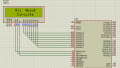
HD44780 Compatible LCD Modules
In a previous article, we discussed the details of the LCD modules that use the HD44780 LCD controller/driver chip. The pinout for these LCD modules is shown in Figure 1.
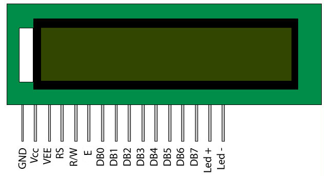
Figure 1. Image courtesy of AAC.
As you can see, there are three control pins (RS, R/W, and E) along with eight data pins (DB7 to DB0). For a write operation, we need to apply appropriate voltages to these pins, as shown in the timing diagram of Figure 2 below.
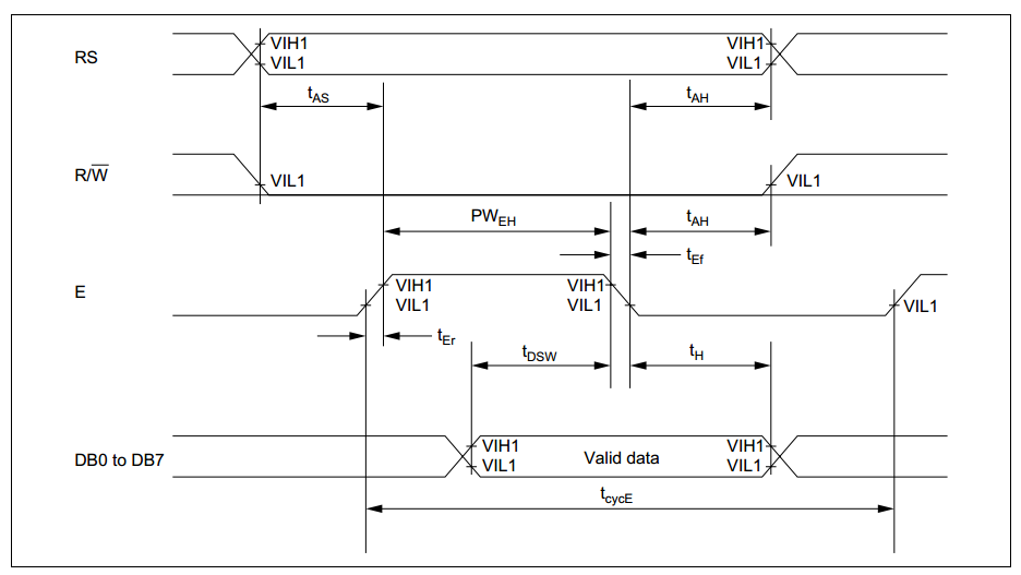
Figure 2. Courtesy of HITACHI.
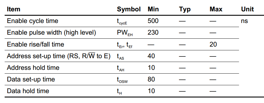
The different delay values of the above timing diagram are given in the following table:
Table 1. Courtesy of HITACHI.
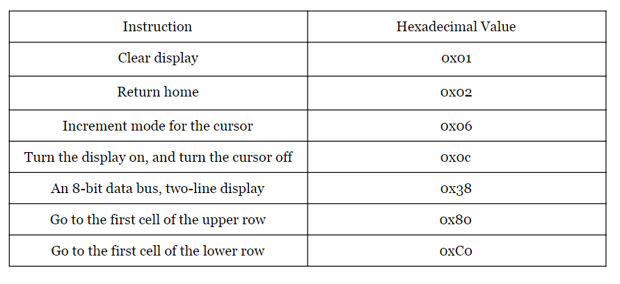
There are several instructions that can be used to configure the LCD module. You can find a complete list of these instructions on page 24 of this datasheet. Some important instructions are listed below.
Table 2
Design Building Blocks: Path 1
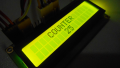
We want to display the message “HELLO WORLD!” on the LCD. Let’s see what building blocks our digital system needs to communicate with the LCD module. We need a ROM to store the ASCII code for the message characters. As shown in Figure 3, the output of the ROM will be connected to the eight data pins of the LCD module.
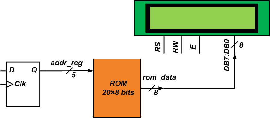
Figure 3
The “HELLO WORLD!” message has 12 characters, and we can use a 12 ✕ 8-bit ROM to store the message. However, let’s consider a 16 ✕ 8-bit ROM for the message so that we can display messages as long as 16 characters (the length of the first row of the LCD).
You may wonder why the above figure shows a 20 ✕ 8-bit ROM if our message is at most 16 characters long. These additional four bytes will be used to store the data related to the LCD instructions that allow us to configure the module. For example, as listed in Table 2, we can apply the hexadecimal value 0x38 to the LCD data pins to specify that the LCD module should receive/send data in 8-bit lengths. Just like the character codes, the hexadecimal values of the commands are applied to the data pins, hence, we can store both of them in the same ROM.
In this article, we’ll use four commands—0x38, 0x06, 0x0C, and 0x01—to configure the LCD. You can find a brief description of these commands in Table 2. For a detailed explanation, please refer to this article. Hence, we have a 20 ✕ 8-bit ROM, where the first four bytes are 0x38, 0x06, 0x0C, and 0x01. The next 16 bytes store the ASCII code for our message.
Considering the timing diagram of Figure 2, we observe that the data applied to DB7-DB0 should not change for a certain amount of time so that the LCD can read it successfully. Hence, as shown in Figure 3, we need a set of D-type flip-flops (DFFs) to keep the ROM address (and consequently, DB7-DB0) constant for some amount of time. After the LCD reads the data, we’ll need to increase the address value by one to apply the next character/command to the LCD. Therefore, as shown in Figure 4, a multiplexer and incrementer should be placed before the DFFs.
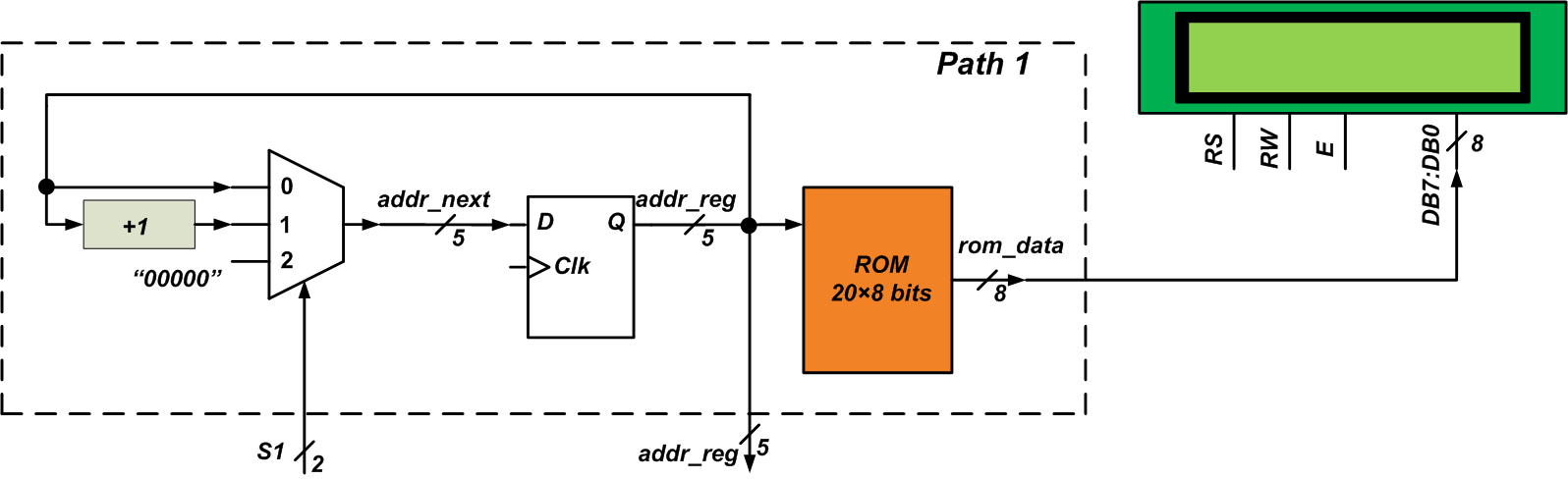
Figure 4
Using the select input of the multiplexer, we can specify whether the address value should remain constant (S1 = 0) or be incremented (S1 = 1). The multiplexer has a third option that allows us to reset the address value to 00000. This can be achieved by resetting the DFFs too. We’ll refer to all these blocks as Path 1, as shown in the figure. As discussed later in the article, we’ll use the S1 signal to control the circuitry inside the Path 1 block. The addr-reg signal will be used to monitor the status of Path 1.
It’s worthwhile to mention that while the above figure shows only one DFF, there are actually five of them (because the 20-byte ROM needs a five-bit address bus).
Design Building Blocks: Implementing the Delays
As discussed above, the waveforms applied to the control inputs of the LCD should follow the timing diagram of Figure 2. After the RW and RS pins change state, we have to wait for tAS before setting the E pin to logic high. Then, a high-to-low transition on E starts a write operation. However, for some amount of time before (tDSW) and after (tH) the falling edge of E, the data should not change.
Therefore, to successfully communicate with the LCD, we have to implement the delays tAS, tDSW, and tH. This can be achieved by a counter. Since we need to sometimes halt the counter or reset it, we’ll put a multiplexer before the DFFs of the counter. This is shown in Figure 5 below.
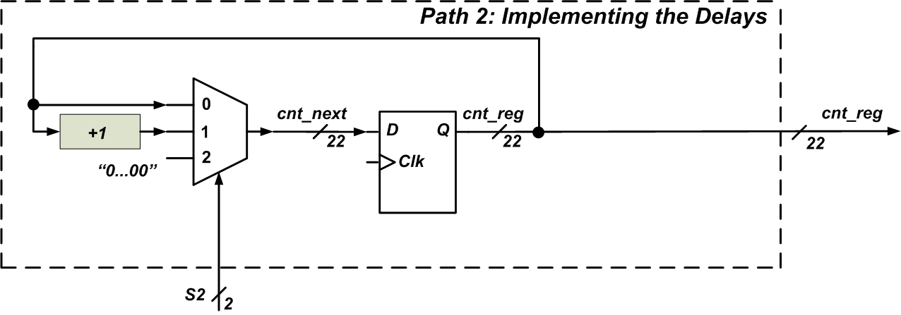
Figure 5
In this way, we can use the S2 input to control the counter and the cnt_reg output will give us the status of the counter, which is an indication of the elapsed time. According to the timing diagram, we need three different time delays: tAS=40 ns, tDSW=80 ns, and tH=10 ns. Noting that the clock frequency of the Mojo V3 board is 50 MHz (a clock period of 20 ns), we can calculate the number of counts required for each time delay.
However, it turns out that my 16x2 LCD needs much longer delays to operate. This is probably due to the fact that I’m using relatively long wires and a breadboard to test my design. In this article, I will implement tAS=10 ms and tH=3 ms. I’ll keep the E signal high for 58ms (PWEH=58 ms). My design should be able to work with delays that are a little bit shorter. You can do some experiments and tweak these numbers for your design.
How many bits do we need for the counter? With the delays chosen, the total delay will be 10+58+3 ms = 71 ms. Considering the clock period of the Mojo (20 ns), a delay of 71 ms can be implemented by counting from 0 up to 3,549,999. Hence, as shown in Figure 5, we need a 22-bit counter.
Design Building Blocks: The Control Path
The final building block that we need is a unit that controls the Path 1 and Path 2 blocks appropriately so that the desired waveforms are generated for the LCD module. This can be achieved by a finite state machine (FSM) that receives addr_reg and cnt_reg signals (the status of Path 1 and Path 2) and generates appropriate s1 and s2 signals. An initial design for this FSM is shown in Figure 6.
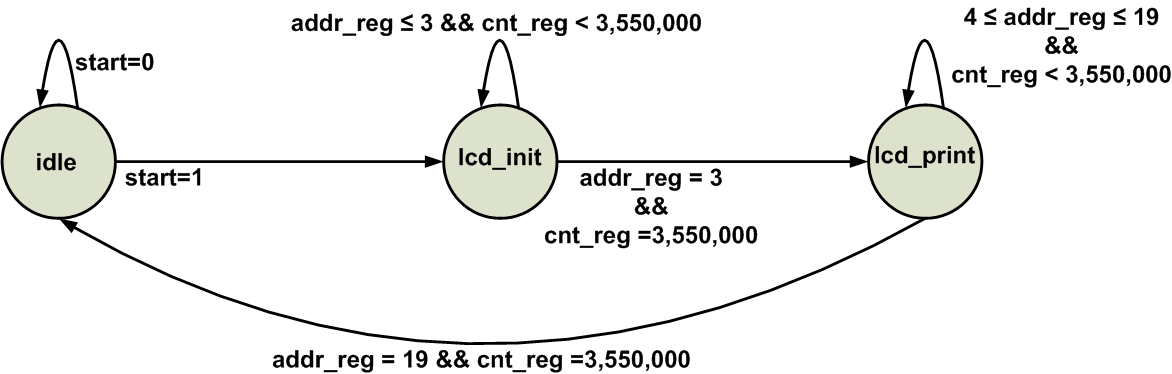
Figure 6
Note that the diagram only shows the state transitions (the outputs of the FSM are not shown). There are three states: during the idle state the signals get their initial values. The lcd_init state applies the LCD configuration commands; that’s why the state transition condition is (addr_reg = 3 && cnt_reg = 3,550,000). In other words, we have four commands, and when the fourth command (addr_reg = 3) is applied to the LCD for 71 ms (cnt_reg = 3,550,000), we should go to the lcd_print state that sends the message data to the LCD. When we reach the end of the ROM (addr_reg = 19), we should wait for 71 ms (cnt_reg = 3,550,000) and then transition to the idle state.
The difficult part of the project is almost done. Now, we just need to design the FSM and write its Verilog code. These tasks will be discussed in the next part of the article.
Conclusion
With FPGAs, we usually have to look at the problem at the lowest level of the design. What we have are logic gates and some basic building blocks such as adders and comparators. Although this makes the FPGA design difficult, FPGAs do offer several advantages. In this article, we examined the building blocks for interfacing an FPGA with a common 16x2 LCD module. A ROM, some DFFs, and multiplexers are required to implement the FPGA-to-LCD interface. Additionally, we need an FSM to control these building blocks. The next article will give the details of designing the FSM and writing its Verilog code. Then, we’ll program the Mojo V3 board to verify our design.
Related Content