 Facebook
 Google
 GitHub
 Linkedin
How to Interface a 16×2 LCD Module with an MCU
This article will discuss the details of interfacing a 16x2 LCD module with an MCU.
This article will discuss the details of interfacing a basic 16x2 LCD module with an MCU.
This article will take a look at the pinout of a basic 16×2 LCD module. Then, it’ll discuss some important instructions for the common LCD modules that are compatible with the HD44780 LCD controller/driver chip. Finally, the article will give an example C code to interface an AVR ATMEGA32 microcontroller with a 16×2 LCD.
The Module Pinout
The 1602A is a 16 character, 2 line display that is similar to many other 16x2 displays in use today. Each character is displayed in a 5 column × 8 row dot matrix or a 5 column × 10 row dot matrix. These pixels should be controlled correctly so that we can display the desired characters. Directly controlling all of these pixels using a microcontroller is not easy, that’s why we usually use LCD modules that have a controller/driver chip to facilitate connecting the LCD to a processor. A common LCD driver is HD44780. The pinout for these LCD modules is usually as shown in Figure 1 below.
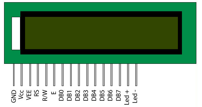
Figure 1. The common pinout for a 16×2 LCD module. Image courtesy of AAC.
The GND and Vcc (+5 V) pins are the power supply pins. The VEE pin is used to adjust the display contrast. We can use a potentiometer to connect VEE to a suitable positive voltage below +5 V. The Led+ and Led- pins are used to turn on the display backlight (connect them to +5 V and ground, respectively).
The RS pin is the Register Selector pin for the LCD controller. The HD44780 has two registers: an Instruction Register (IR) and a Data Register (DR). The RS pin is a control pin that specifies whether the IR or DR should be connected to the Data Bus (DB0 to DB7 pins). When RS is low, the IR is selected and DB7-DB0 are treated as an instruction code. For example, the instruction code can represent a “display clear” command. When the RS is high, the DR is selected and DB7-DB0 are treated as data. In this case, DB7-DB0 can be the code for representing a character such as “a”.
The R/W pin specifies whether we are writing to the module (R/W=0) or reading from it (R/W=1).
The E pin (for “Enable”) starts a read/write operation and will be discussed in the next section.
The Timing Diagram for a Write Operation
Although we can both write and read from the data bus, a write operation is more common. That’s why, in this section, we’ll examine the timing diagram of a write operation which is shown in Figure 2 below. The definition of the different parameters and the expected values are given in Table 1.
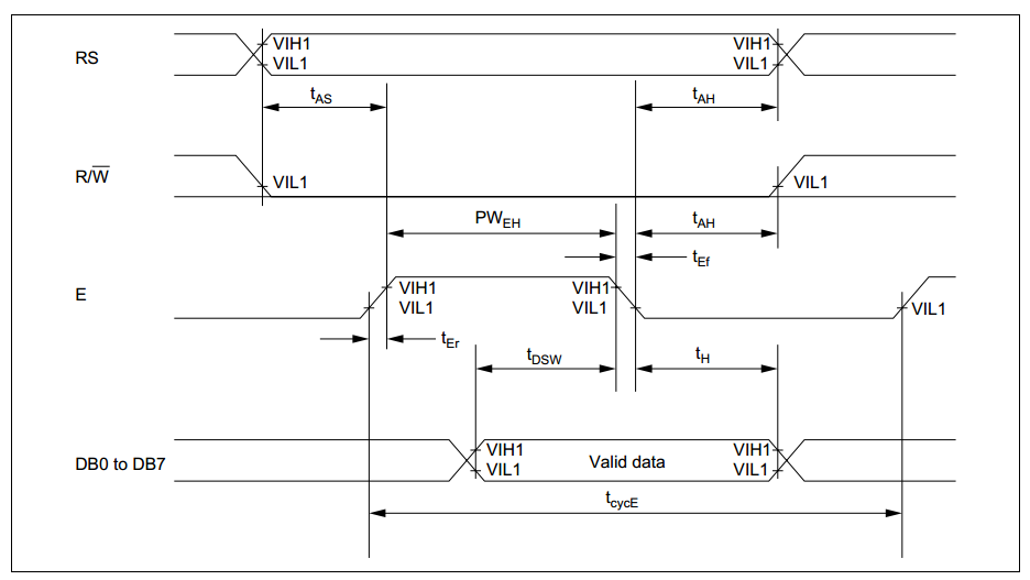
Figure 2. Timing diagram of a write operation. Image courtesy of HITACHI.
Table 1 Courtesy of HITACHI.
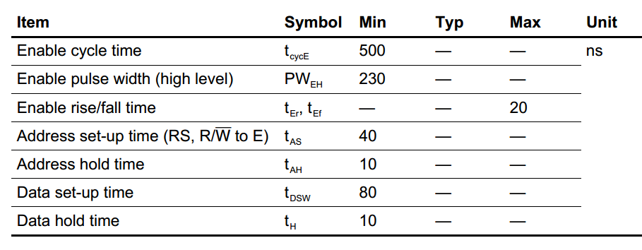
The timing diagram shows that we should set the RS and R/W pins to appropriate values and wait for tAS( which should be greater than 40 ns) before setting the E pin to logic high. According to the table, the E signal should have a width (PWEH) greater than 230 ns.
Then, the E signal should have a high-to-low edge which starts a write operation. Note that tDSW before this edge the data must be valid. Besides, after the falling edge of E, the control signals and the data should not change for some time denoted by tAH and tH in the figure. Another important issue is the “Enable Cycle Time” which should be greater than 500 ns. This shows that we should wait for some time before starting to do the next read or write operation.
To summarize, a high-to-low transition on E starts data read or write but there are certain timing conditions that must be met. When interfacing the LCD module with an MCU, we’ll have to take these considerations into account.
Important Instructions
You can find the complete list of the instructions for an HD44780-compatible LCD module on page 24 of this datasheet. Here, we’ll only use some of these instructions to do some basic operations.
Clear Display
This instruction clears the display. You’ll have to set both RS and R/W to the logic low and perform a write operation which applies the hexadecimal value 0x01 to the data bus. Moreover, the datasheet states that the “clear display” command “sets DDRAM address 0 in the address counter”. What does this mean?
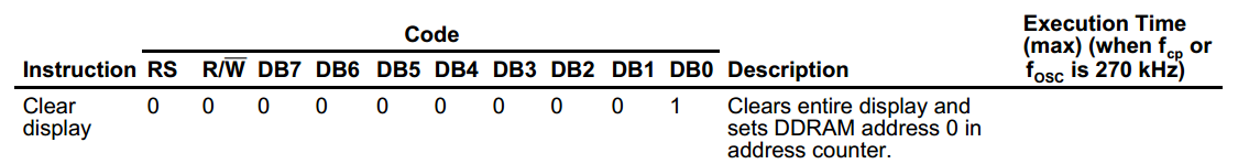
Figure 3. Courtesy of HITACHI.
The Display Data RAM (DDRAM) is a RAM that stores the ASCII code for the characters that we send to the LCD module. The DDRAM can store up to 80 characters (it has a capacity of 80×8 bits). However, only some of these 80 characters are displayed on the LCD. For example, in the case of a 16×2 LCD, only 32 of these memory locations are displayed. The relationships between the displayed DDRAM addresses and the LCD positions are shown in Figure 4.
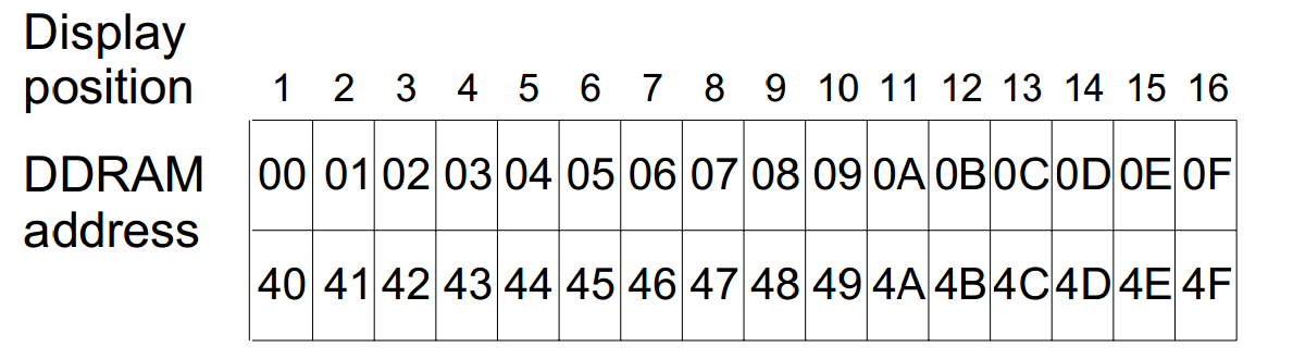
Figure 4. Courtesy of HITACHI.
According to Figure 4, if we write a particular character to the DDRAM address 0x00, it will be displayed in the first cell of the upper line. Similarly, if we write a character to address 0x40, that will appear in the first cell of the lower line.
To go to a particular address of the DDRAM, we can write the desired address to the Address Counter (AC). Moreover, the AC determines the position on the LCD that a character entered by a write operation goes to.
Note that LCDs support shift operations that can change the relationships that were shown in Figure 4. For example, a left shift applied to the default status of Figure 4 will lead to Figure 5. For more information, please refer to the datasheet.
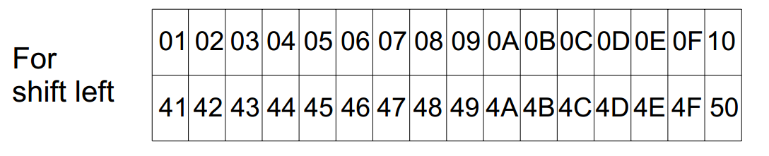
Figure 4. Courtesy of HITACHI.
Now that you’re familiar with the DDRAM and AC, the description of the “Clear Display” command should make sense to you. The “Clear Display” command “sets DDRAM address 0 in the address counter”, hence, it will return the cursor to the home position (the first cell of the upper line).
Return Home
Figure 6 gives the code for this command and its description.
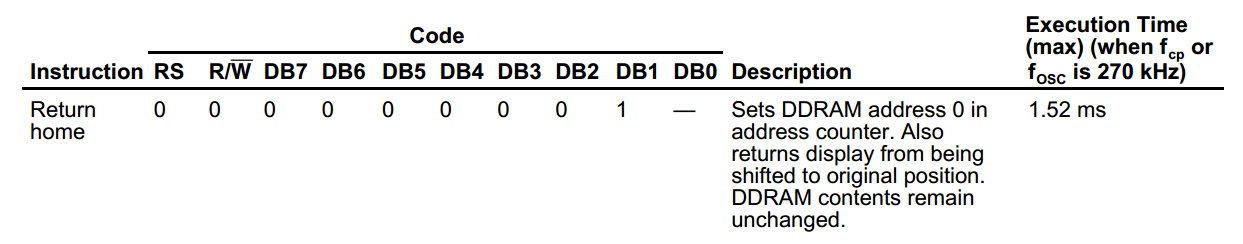
Figure 6. Courtesy of HITACHI.
This command also brings the cursor back to the home position and returns the display to its original status if it was shifted. For this command, DB0 is a don’t-care.
Entry Mode Set
The details of this command are given in Figure 7.
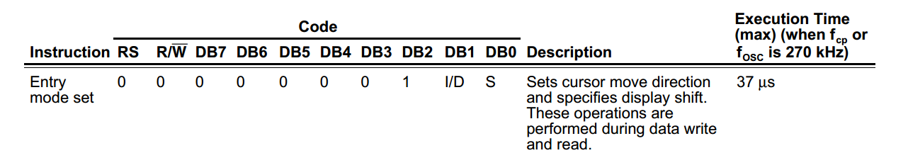
Figure 7. Courtesy of HITACHI.
When “I/D” is 1, the cursor position is incremented by one (it moves to the right on the display) after a write operation. When “I/D” is 0, the cursor position is decremented by one (it moves to the left).
The S bit specifies whether to shift the display or not (A shift changes the DDRAM addresses that are displayed on the LCD). When S is 0, the display does not shift. For the shift options (when S=1), please refer to the datasheet.
In many cases, we want the cursor position to increment after a write operation while the display remains still (the shift option is not utilized). For such applications, the command code for DB7-DB0 will be the hexadecimal value 0x06.
Display ON/OFF Control
The details of this command are given below.
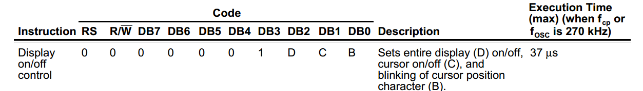
Figure 8. Courtesy of HITACHI.
By setting the D bit to 1 or 0, we can respectively turn the display on and off. Similarly, the C bit can be used to turn the cursor on/off. B controls the blinking capability of the cursor position. Hence, if we write the hexadecimal value 0x0C to the DB7-DB0 as an instruction, the LCD will turn on and the cursor will be off.
Function Set
The following figure gives details of the “Function Set” command.
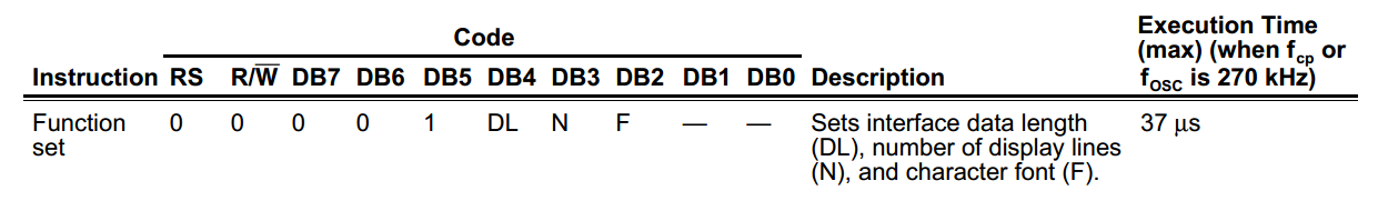
Figure 9. Courtesy of HITACHI.
The DL bit specifies the data length for the LCD module. If DL=1, the data is sent and received as an 8-bit word on the data bus (DB7 to DB0). When DL=0, the data is sent and received in 4-bit lengths (DB7 to DB4). To keep things simple, we’ll use the 8-bit option in this article.
The N bit specifies the number of display lines. For a single line display, N should be 0. For two lines and more, N should be 1.
“F” determines the character font and most often is 0.
Hence, when working with a 16×2 LCD that receives and sends data in 8-bit lengths, the “Function Set” code for DB7-DB0 will be the hexadecimal value 0x38.
Set DDRAM Address
This instruction sets the address of the DDRAM. It can be used to write a character in a particular cell of the LCD. For example, sending the hexadecimal value 0x80 to the data bus will make the cursor to move to the first cell of the upper row.
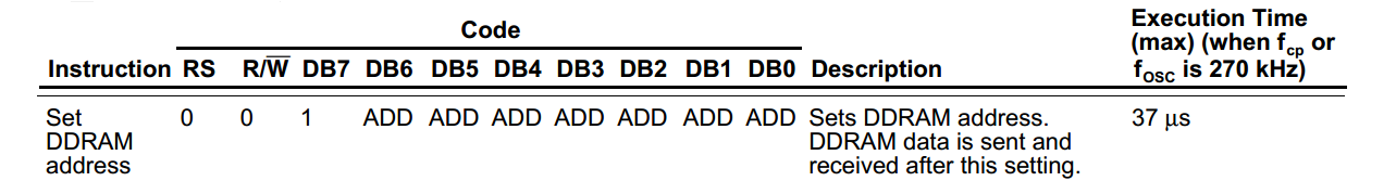
Figure 10. Courtesy of HITACHI.
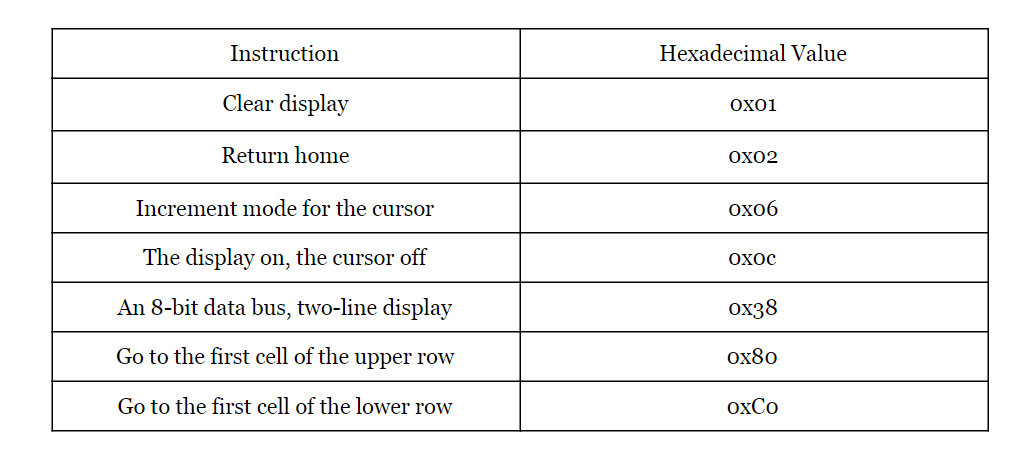
Now, we will use the above commands to operate a 16×2 LCD. The following table summarizes the commands discussed above.
Table 2
Interfacing the LCD with an AVR
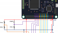
Now, we will write some functions to connect a 16×2 LCD to a ATMEGA32. Assume that, as shown in Figure 11, port A is connected to the LCD data bus and the first three pins of port B are used to control the RS, RW, and E pins of the LCD. Note that the connections for the VSS, VDD, and VEE are not shown in Figure 11.
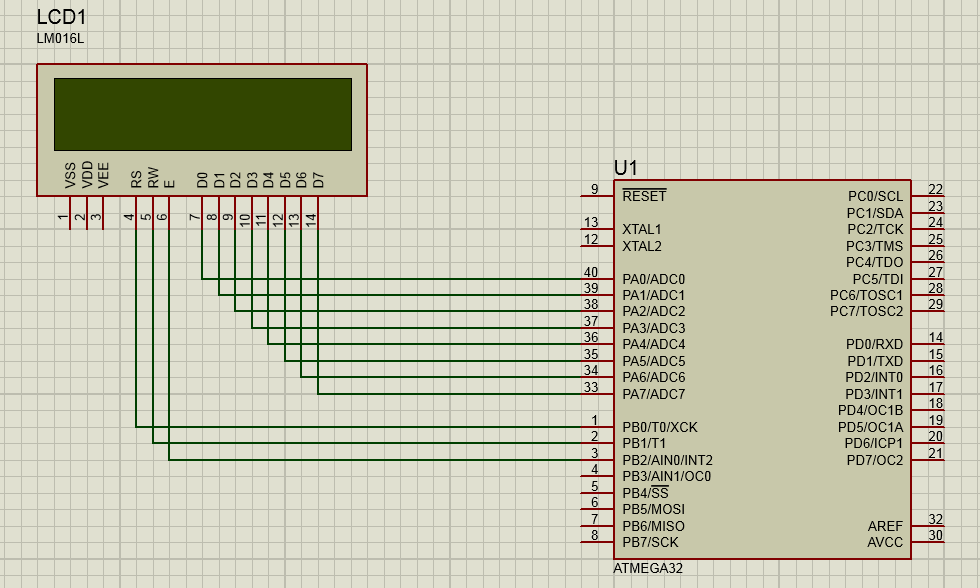
Figure 11
We need two functions to write commands and data to the LCD module. Before that, let’s define the following three constants:
const unsigned char     RS_Pin=0x01;
const unsigned char     RW_Pin=0x02;
const unsigned char 	E_Pin=0x04;
These constants will be used throughout the code to specify the PORTB pin numbers that are connected to the control pins of the LCD. For example, RS is connected to the first pin of port B in Figure 11 so the RS_Pin is 00000001. E is connected to the 3rd pin so E_Pin is 00000100. In this way, we can easily modify the constants to adapt the code for a future project that uses a different pin connection. We can send instructions to the LCD using the following function:
void lcd_write_instruc (unsigned char instruc)
	{
    	delay_ms(2);
    	PORTB=PORTB & (~(RS_Pin));      	//it is an instruction rather than data
    	PORTB=PORTB & (~(RW_Pin));      //it is write operation
    	PORTB=PORTB & (~(E_Pin));       	//set E to 0 (see Figure 1)
    	PORTA=instruc;                    		//put the instruction on the data bus
    	PORTB=PORTB | (E_Pin);            	//set E to 1 (see Figure 1)
    	PORTB=PORTB & (~(E_Pin));       	 // set E to 0 to generate a falling edge
	}
Here, “instruc” is the command code that must be sent to the LCD data bus. The first line of the code uses the delay_ms() function from “delay.h” library to introduce a delay of 2 ms. We need to give the LCD some time to finish its current job (if there is any). This delay is introduced to take the “Enable Cycle Time” constraint of Figure 2 into account. Similarly, we can write a function to send a character to the LCD:
void lcd_write_char (unsigned char c)
	{
    	delay_ms(2);
    	PORTB=PORTB | (RS_Pin);        //it is data rather than an instruction
    	PORTB=PORTB & (~(RW_Pin));
    	PORTB=PORTB & (~(E_Pin));
    	PORTA=c;
    	PORTB=PORTB | (E_Pin);
    	PORTB=PORTB & (~(E_Pin));
	}
“c” is the data that must be sent to the LCD data bus. The following function initializes the LCD by sending some commands from Table 2. It also specifies PORTA and PORTB of the MCU as outputs.
void lcd_init (void)
	{
    	delay_ms(2);
    	DDRA=0xFF;
    	DDRB=0xFF;
    	lcd_write_instruc(0x06);        //Increment mode for the cursor
    	lcd_write_instruc(0x0C);        //The display on, the cursor off
    	lcd_write_instruc(0x38);        //An 8-bit data bus, two-line display
	}
The following function clears the display:
void lcd_clear(void)
{
delay_ms(2);
lcd_write_instruc(0x01);        //Clear the display
lcd_write_instruc(0x02);        //returns the display to its original status if it was shifted.
}
To set the AC to a given address, we can use the following function:
void lcd_goto(unsigned char column, unsigned char row)
	{
	delay_ms(2);
	if(row==0)
	lcd_write_instruc(0x80 + column);		//see Figures 4 and 10
	if(row==1)
	lcd_write_instruc(0xC0+ column);		//see Figures 4 and 10
	}
And, finally, to write a string of characters, we can successively use our lcd_write_char() function:
void lcd_write_string(char *s)
	{
	delay_ms(2);
	while(*s != 0)
	{
	lcd_write_char(*s);
	s++;
	}
	}
Using these functions we can have the basic functionality of the LCD module. The following code shows the main() function of an example:
void main(void)
{


        lcd_init();
        lcd_clear();
        lcd_goto(0,0);
        lcd_write_string("    All  About   ");
        lcd_goto(0,1);
        lcd_write_string("     Circuits   ");
while (1)
    {
        continue;
    }
}
The output of the above code compiled and simulated using CodeVision and Proteus tools is shown in Figure 12.
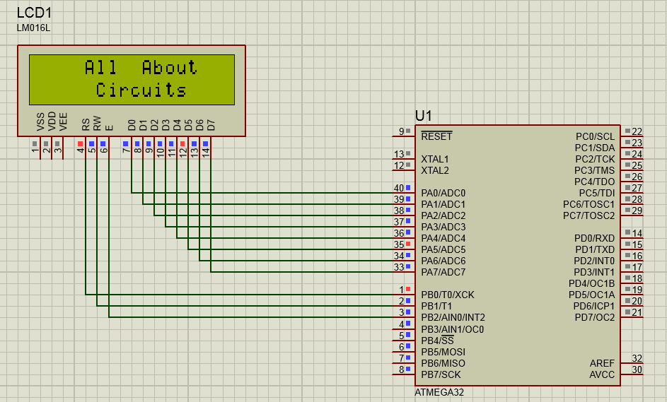
Figure 12
It’s worth to mention that the MCU delay to perform the different lines of the above code provides sufficient delay to satisfy the different timing constraints of Figure 2 particularly those related to the E signal. In fact, I have used the above functions with even faster 32-bit MCUs but if you run into any trouble, you can introduce a small delay in the appropriate lines of the code to make sure that the timing requirements are met.
In this article, we looked at the pinout of a basic 16×2 LCD module. We also examined some of the most important instructions for the HD44780 compatible LCD modules. The example C code given in the article can be adjusted to be used with MCUs from other vendors.
To see a complete list of my articles, please visit this page.
Related Content


In the section titled “Interfacing the LCD with an AVR” when assigning the E_Pin to a pin value doesn’t make sense to me, “E is connected to the 3rd pin so E_Pin is 00000100”. Shouldn’t it be “E_Pin is connected to the 3rd pin on the Atmega32 so E_Pin is 00000011” and the code should be “const unsigned char =0x03”. Please advise.
Great tutorial, it provides just enough information to make me curious.
Copying and pasting this code directly into AVR Studio 7 requires minor changes to the code. Most of the time was spent configuring AS7 to work with Sparkfun’s AVR pocket programmer.
Instructions can be found here :
1. https://medium.com/jungletronics/how-to-load-programs-to-an-arduino-uno-from-atmel-studio-7-83c8dd8d175d
2. http://www.microdigitaled.com/AVR/Hardware/Arduino/UsingArduinoBoardsInAtmelStudio.pdf
https://www.arnabkumardas.com/platforms/atmel/how-to-flash-or-program-arduino-from-atmel-studio/
3. https://www.arnabkumardas.com/platforms/atmel/how-to-flash-or-program-arduino-from-atmel-studio/
I had no success with RS_Pin, RW_Pin, and E_Pin as const unsigned chars assigned to 0x01, 0x02, or 0x03.
I bit-twiddled (bit shifting) instead of bit masking.
I used PB0, PB1, and PB2 for RS_Pin, RW_Pin, and E_Pin and PD0-PD7 for D0-D7 on the LCD respectively.
For example change the following from the write_char function:
PORTB=PORTB & (~(RS_Pin));—> to PORTB=PORTB & (~(1<<0)); // clearing PB0 bit of PORTB aka RS_Pin
PORTB=PORTB & (~(RW_Pin));—> to PORTB=PORTB & (~(1<<1)); // clearing PB1 bit of PORTB aka RW_Pin
PORTB=PORTB & (~(E_Pin));—> to PORTB=PORTB & (~(1<<2)); // clearing PB2 bit of PORTB aka E_Pin
Anywhere there is reference to the const unsigned chars replace with the shift operations.
You can then comment out the const unsigned chars.
In the code provided by this tutorial, the function delay_ms() needs to have a leading underscore. So change all delay_ms() to _delay_ms(). The leading underscore is to signify internal library use, i.e. delay.h.
Lastly, define the CPU frequency as such in this order:
#include <a>
#define F_CPU 16000000UL
#include “util/delay.h”
Have fun.