 Facebook
 Google
 GitHub
 Linkedin
How to Simulate a Phase-Locked Loop
This article presents an LTspice circuit that can be used to explore the behavior of a phase-locked loop.
This article presents an LTspice circuit that can be used to explore the behavior of a phase-locked loop.
In a previous article I introduced the fundamental concepts and the core functionality of a negative-feedback system known as a phase-locked loop (PLL). As you may recall, the most basic PLL consists of a phase detector (actually a phase difference detector), a low-pass filter, and a voltage-controlled oscillator:
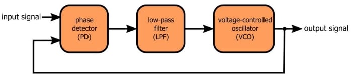
The periodic waveform produced by the VCO is the primary output signal. Under the right circumstances, a PLL will ensure that the frequency of the output signal is exactly equal to the frequency of the input signal.
I prefer to perform simulations myself rather than rely completely on plots and equations and explanations created by someone else. This applies to just about any circuit, but it is especially important with PLLs because analytical exploration of PLL functionality is, in my opinion, confusing and inadequate.
This is especially true with the initial transient response, i.e., the behavior exhibited by the PLL when it is attempting to lock onto an input signal. The transient response of a PLL is not only elusive when we try to achieve an intuitive understanding—it is also nonlinear and not easily translated into equations. In fact, the abstract of this academic paper indicates that even “accurate numerical simulations” can be problematic because they require so much processing time.
The Circuit
There are many ways in which you could simulate a PLL. There is nothing particularly special about the circuit that I created, but I think it’s a good place to start, for two reasons: it’s conceptually simple and it doesn’t overburden the SPICE engine (in other words, there’s no need to take a coffee break while you’re waiting for the simulation to finish).
This is my LTspice PLL:
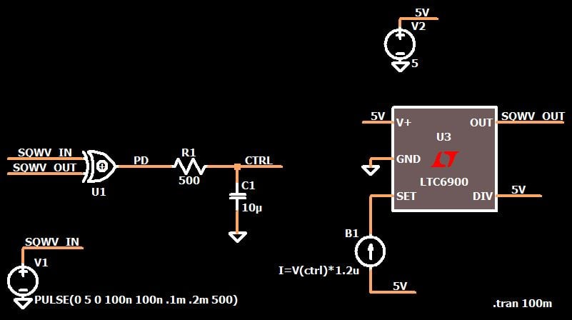
Two of the three functional blocks are very straightforward. The phase detector is an XOR gate (I’m using the library discussed here), and the low-pass filter is a single-pole RC circuit. From what I understand, even professional-quality PLLs can often achieve adequate performance with nothing more than an RC low-pass. I tried a second-order filter in my simulation, and the RC circuit worked better. It seems to me that the additional ripple suppression provided by a second-order filter is simply not necessary.
The VCO
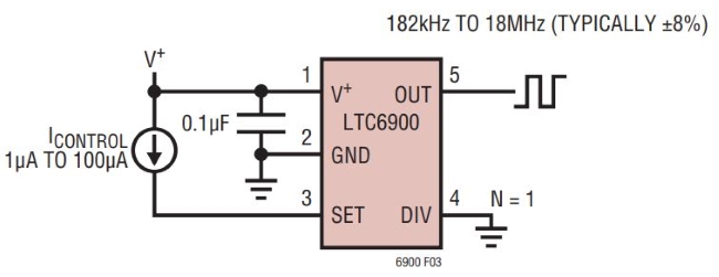
The less-straightforward portion of the system is the VCO block. Instead of a custom-designed circuit such as a variable-frequency Colpitts oscillator, I decided to save myself some serious time and energy by using a macromodel for a Linear Tech resistor-set oscillator IC.
The LTC6900 supports frequencies from 1 kHz to 20 MHz. Despite the fact that it is called a “resistor-set” oscillator, you can also control the frequency by directly adjusting the amount of current flowing into the SET pin. This is not surprising, since the resistor (connected between SET and V+) is simply a means of establishing the current flowing into the SET pin, which is held by internal circuitry at the V+ voltage minus ~1.1 V.
As you can see, my LTC6900 implementation is similar:
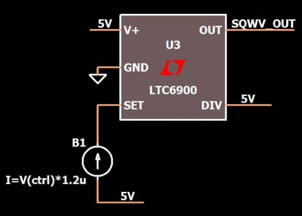
The first difference is that the DIV pin is at 5 V instead of ground (because I wanted lower frequencies). The other change that I made (not surprising considering the objective here) is that instead of a fixed current source I have a voltage-controlled current source. This is the most subtle portion of the circuit, so let’s take a closer look.
From Voltage to Current to Frequency
The low-pass-filtered phase detector signal serves as the control voltage for the VCO. I have simplified my circuit by using a mathematical relationship, instead of components, to translate from control voltage to control current. The current flowing into the SET pin is defined (using an arbitrary behavioral current source) as the voltage at the CTRL node multiplied by a constant.
The next step is to determine the constant. We know that our input frequency is 5 kHz, and consequently the VCO will eventually need to settle on an output frequency of 5 kHz. Through trial and error I determined that the VCO will generate a 5 kHz waveform when the current flowing into the SET pin is around 2.9 µA. This is the first thing we need to know.
Next we need to consider the control voltage. The output from the phase detector switches between ground and 5 V, which means that the control-voltage range is also 0 to 5 V. We need to make sure that the control voltage corresponding to a SET-pin current of ~2.9 µA will be somewhere within the range 0–5 V. And actually, I want the final control voltage to be somewhere near the middle of the range, i.e., 2.5 V. Thus, I simply divide 2.9 µA by 2.5 V to determine the factor that will relate the SET-pin current to the control voltage.
$$\frac{2.9\mu A}{2.5\ V}=1.16\frac{\mu A}{V}\approx\ 1.2\frac{\mu A}{V} \ \ \Rightarrow\ \ I=(V_{CTRL})(1.2\times10^{-6})$$
Another thing to keep in mind is that the VCO should be compatible with the current that will be generated when the control voltage is at its maximum value. We can’t really predict the circuit’s startup behavior, so we might as well assume that differences between the phase of the input and output signals (or some other initial condition) could lead to high phase-detector duty cycles and, consequently, high control voltages. If these high control voltages cause the VCO to malfunction, we’ll be in trouble. In my LTspice circuit, VCTRL of 5 V leads to SET-pin current of 6 µA, which is well within the acceptable range.
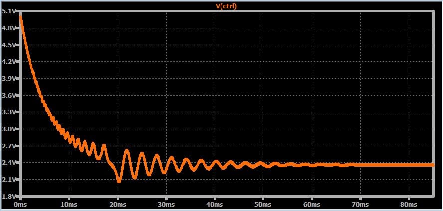
We’ll examine simulation details and results in a future article. For now I’ll leave you with the following plot, which shows the variations in control voltage as the PLL gradually locks onto the input frequency.
Conclusion
In this article I presented and explained the LTspice circuit that I designed for performing straightforward phase-locked loop simulations. The transient response is evident in the plot of the control voltage (i.e., the low-pass-filtered output of the phase detector). We’ll continue our SPICE-based PLL experimentation in the next article.
Feel free to download my LTspice schematic by clicking on the orange button.


It’s very good. instead you to proceeding write, I proceed to read and learn. thanks for your knowledge.