 Facebook
 Google
 GitHub
 Linkedin
Introduction to CMOS Image Sensors
In this article, you'll learn the basics of the CMOS image sensor, including its core components, its block diagram, its strengths and weaknesses, and its applications.
An image sensor is one of the main building blocks in a digital imaging system and strongly influences the overall system performance. The two main types of image sensors are charge-coupled devices (CCD) and CMOS imagers. In this article, we’ll take a look at the basics of CMOS image sensors.
Check out our series on charge-coupled device (CCD) image sensors. You can start with the structure and functionality of CCDs.
CMOS Photo-Detectors
Most CMOS photo-detectors are based on the operation of a PN-junction photodiode. When a photodiode is reverse-biased (and the reverse voltage is less than the avalanche breakdown voltage), a current component proportional to the incident light intensity will flow through the diode. This current component is often referred to as photo-current.
Since the photo-current linearly increases with light intensity, we can use a photodiode to build a photo-detector. An abstract representation of such a photo-detection structure is shown below.
![]()
(a) Schematic of an example photo-detector (b) Change vs. time for photo-current values. Image courtesy of Abbas El Gamal.
The reset switch is closed at the beginning of an exposure cycle to reverse-bias the photodiode to a voltage of VD. Next, the switch opens and a photo-current proportional to the incident light intensity is generated. This current is in the range of femto- to pico amperes and is too small to be directly measured. If we let the photodiode be exposed to the light for a set period of time, tint, the current will be integrated over the diode capacitance CD. The stored charge provides us with a stronger accumulated signal that is easier to measure. Besides, the averaging process incorporated makes the accumulated signal a more faithful representation of the measured light intensity especially when dealing with weak or noisy signals.
Note that the well capacity, Qwell, sets an upper limit for the amount of charge that CD can hold. Above a certain light intensity, the diode will be saturated and the accumulated charge will be equal to a maximum value as shown in the above figure. Hence, the integration period must be chosen carefully.
Another non-ideal effect that should be considered is that, in addition to the photo-current, there is another current component called dark current that flows through the diode. The dark current is the current that is generated in the absence of light. This current component must be minimized to maximize the device sensitivity.
Block Diagram of a CMOS Image Sensor
The basic structure of a CMOS image sensor is depicted below.

Image courtesy of Edmund Optics.
A two-dimensional array of photo-detectors is used to sense the incident light intensity. The charge created by a photo-detector is converted to a voltage signal and passed on to the output amplifier through an array of “row select” and “column select” switches. An ADC is used to digitize the amplified signal.
To perform readout, the pixel values of a given row are transferred in parallel to a set of storage capacitors (not shown above) and then, these transferred pixel values are read out sequentially.
The above figure shows an APS (active-pixel sensor) architecture. In an APS device, each pixel location contains not only the photodiode but also an amplifier. A simpler architecture, known as PPS (passive-pixel sensor), does not integrate an amplifier into the pixel. In a DPS (digital-pixel sensor) device, each pixel has its own analog-to-digital converter and memory block. Hence, the pixels in a DPS architecture output digital values proportional to light intensity.
![]()
The schematic of a DPS or diagram pixel sensor. Image courtesy of Abbas El Gamal.
Pros and Cons of CMOS Image Sensors
As the name suggests, CMOS image sensors are fabricated in a standard CMOS technology. This is a major advantage because it allows us to integrate the sensor with other analog and digital circuits required for an imaging system. An integrated solution allows us to reduce the power consumption and improve the readout speed. This is not the case with other image sensor technologies such as charge-coupled devices (CCD) that are based on special-purpose fabrication technologies optimized for charge transfer and imaging.
A drawback to a CMOS image sensor is that there are several active devices in the readout path that can produce time-varying noise. Besides, fabrication inconsistencies can lead to mismatch between charge-to-voltage amplifiers of different pixels. This results in fixed-pattern noise, where different pixels produce different values even though they are exposed to uniform illumination.
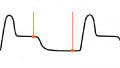
Rolling Shutter Artifacts
With many CMOS image sensors, the exposure cycle of different pixel rows start at slightly different times. Typically, the rows are reset in sequence from top to the bottom. After the integration time of a given row passes by, its readout should start. Hence, light integration happens in sequence from top to the bottom just like the reset process. This can cause a kind of distortion called rolling shutter artifact when capturing a fast-moving object. This is due to the fact that a scene with a fast-moving object can change by the time all of the pixels are captured. Rolling shutter artifact manifests itself as some non-rigidity or bending in the captured scene. This is illustrated in the following figure.

Image courtesy of ON Semiconductor.
Modern higher-end CMOS sensors have much faster readout rates and can more easily avoid this non-ideal effect. Besides, there are CMOS image sensors with a global shutter, where the reset and exposure cycle of all of the pixels happen at the same time. At the end of the integration time, the accumulated charge of different pixels is simultaneously transferred to a storage area for further processing. Since the exposure cycle of all of the pixels occurs at the same time, there will be no rolling shutter effect.
Conclusion
A reverse-biased photodiode produces a current component that is proportional to the incident light intensity. A two-dimensional array of these photo-detectors can be used to implement a CMOS image sensor. The pixels in a CMOS image sensor can have different levels of complexity. For example, pixels of a CMOS image sensor can contain not only the photodiode but also an amplifier. A DPS (digital-pixel sensor) device employs more complex pixels where each pixel has its own analog-to-digital converter and memory block.
The most important advantage of CMOS image sensors is the possibility of integrating the sensor with other analog and digital circuits required for an imaging system. Two noise sources that can degrade the performance of CMOS image sensors are the fabrication mismatch between components of different pixels and the noise from active devices in the readout path.
Related Content


can somebody tell me what this means?
“When a photodiode is reverse-biased, a current component proportional to the incident light intensity will flow through the diode…. Next, the switch opens and a photo-current proportional to the incident light intensity is generated.”