Facebook
 Google
 GitHub
 Linkedin
Introduction to Lossy Transmission Lines
This article will help you understand losses in high-frequency transmission lines that include traces on PCBs. We will also investigate how these losses impact signal propagation and the quality of digital signals.
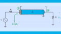
The term "transmission line” is used to distinguish the complicated behavior of signal propagation at high frequencies from ordinary low-frequency interconnect. At high frequencies, complex equations are required to understand the behavior of simple interconnects. A transmission line can be modeled by dividing the line into elements of infinitesimal length where each element itself is modeled as a network of an inductor, a capacitor and two resistors (Figure 1).
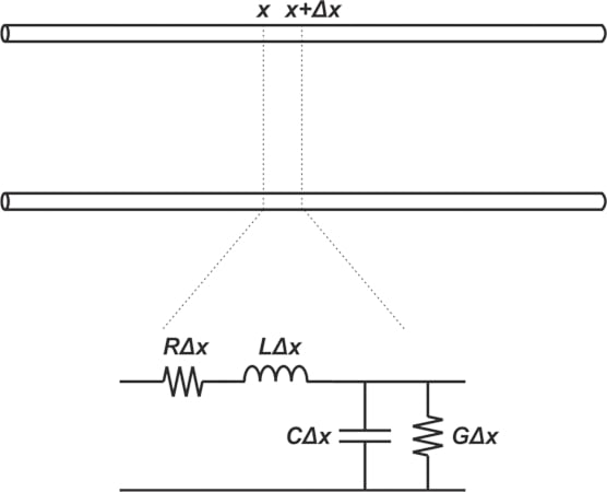
Figure 1. Modeling of a transmission line using RLC components
In a previous article covering the RF design basics of transmission lines, we thoroughly examined the behavior of a lossless line (R=G=0). Losslessness can be a reasonable assumption in many applications because at high frequencies, the inductor’s reactance is usually much greater than the series resistance R and the capacitor’s reactance is usually much less than the shunt resistance. Despite this, there are many applications where the loss of the transmission lines should be taken into account.
For instance, it might be required to send USB signals down a 12-inch path in a large system like a laptop or desktop PC. This long path can result in a lot of loss that can severely distort data and lead to system failure. Understanding lossy transmission lines can be valuable in the design of both high speed digital boards and RF applications.
In the next few articles in this series, we’ll take a look at the major loss mechanisms in transmission lines, but before diving in too far, this article aims to paint a qualitative picture of the behavior of lossy lines and how sinusoidal and square wave signals change as they travel along a lossy line.
Equations of a Lossy Line
We can derive the voltage and current equations following a similar procedure as used for the lossless line. For a lossy line, the complex characteristic impedance Z0 and the complex propagation constant γ are shown in Equations 1 and 2 below:
\[Z_0 =\sqrt{\frac{R+jL \omega}{G+jC \omega}}\]
Equation 1.
\[\gamma = \alpha + j \beta = \sqrt{(R+jL \omega)(G+jC \omega)}\]
Equation 2.
The real part of γ is called the attenuation constant ⍺ (in nepers per meter); and the imaginary part is referred to as the propagation constant β (in radians per meter). If the line is along the x-axis, the forward-traveling voltage wave can take on the form:
\[v(x,t)= A e^{-\alpha x} cos(\omega t-\beta x)\]
Equation 3.
where A is a constant that can be found from boundary conditions at the input and output ports of the line. One major difference between the lossy and lossless case is the exponential term e-⍺x, which shows that the signal gets attenuated as it travels along the lossy line. To get a sense of the attenuation effect on the signal, let’s look at some typical waveforms.
Comparing Lossless and Lossy Lines: Sinusoidal Input
Consider applying a sinusoidal input Vscos(⍵t) with a source impedance of Rs to a load impedance RL through a 40 inch long transmission line (Figure 2(a)). Assume that there is no reflected wave and the forward wave is given by Equation 3.
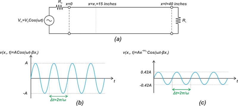
Figure 2. Sinusoidal signal propagation through a lossy transmission line
At a fixed position x=x1 along the line, the βx term in Equation 3 is a constant phase term and the voltage equation is simply a sinusoidal function of time. For a lossless line (⍺=0), the amplitude of this sinusoidal function is constant and equal to A regardless of the value of x. Therefore, at an arbitrary position x, the waveform has an amplitude of A, as shown in Figure 2(b).
For a non-zero value of ⍺, however, the amplitude of the signal reduces along the line. For example, if the line’s loss is 0.5 dB per inch, the total attenuation at a distance of x1=15 inches is 7.5 dB. Therefore, the voltage amplitude at x1=15 inches is:
\[\begin{eqnarray}
Amplitude \ at \ x_1 &=& 10^{\frac{-7.5}{20}} \times A \\
&=& 0.42 A
\end{eqnarray}\]
Figure 2(c) shows the voltage waveform for this lossy line. Now let’s examine the waveform dependency on position by looking at the waveform at a particular instant in time t=t1. In this case, the term ⍵t turns into a constant phase term. For a lossless line (⍺=0), the voltage signal becomes a sinusoidal function of position x, as illustrated in Figure 3(a).
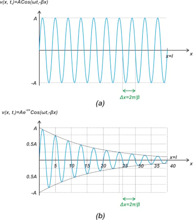
Figure 3. Sinusoidal signal amplitude for lossless and lossy transmission lines
In Figure 3(a), the voltage level changes at different points along the line but the amplitude of variation is constant and equal to A for all values of x. This is in contrast to the lossy case, depicted in Figure 3(b). In this figure, it is assumed that the line has a 0.5 dB/inch attenuation. As we move away from the signal source, the amplitude of the sinusoidal waveform reduces exponentially (due to the e-⍺x term). Note that the line attenuation increases linearly with length. For example, if the attenuation per length of a line is 0.1 dB/inch, the attenuation at the end of a 5 inch long line would be 0.5 dB. The question to be asked now is, how is a square wave affected by a lossy line?
Lossy Lines Increase Rise Time of Digital Signal
It’s important to realize that the transmission line losses increase with frequency. Figure 4 shows the attenuation of two 5-mil wide PCB traces built using a typical FR4 substrate. The figure shows attenuation versus frequency for two different lines: one being 5 inches long (blue) and the other 10 inches long (red).
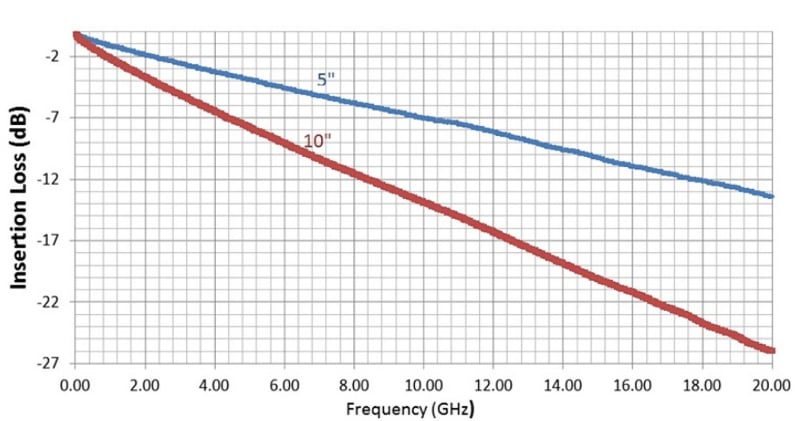
Figure 4. Attenuation (insertion loss) as a function of frequency and trace length. Image used courtesy of TI.
As can be seen, the attenuation has a low-pass characteristic and increases with frequency. A digital signal ideally has abrupt transitions from one logic level to the other. A sharp transition in the time domain corresponds to high frequency components in the frequency domain. For example, a 50% duty cycle square wave with zero rise/fall time has all of the odd harmonics of its fundamental frequency. In other words, a square wave with zero rise/fall time has infinite bandwidth. When this ideal square wave propagates down a lossy line, its high frequency components are inevitably attenuated by the low-pass characteristic of the line. Due to these suppressed high frequency components, the signal rise/fall time increases as it travels down the lossy line. Figure 5 shows how the signal rise time increases along a lossy line.
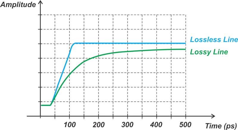
Figure 5. Signal rise time comparison for lossless and lossy transmission lines
Note that as the square wave travels down the line, its amplitude decreases and its rise time increases. In most cases, the increase in the rise time is more detrimental to the signal integrity of the transmitted signal than is the loss in amplitude. To learn how we can quantify the increase in the rise time, please refer to this article.
Rise Time Degradation Leads to Intersymbol Interference
Figure 6 below shows how a long rise and fall times can affect a bit stream in a digital system.
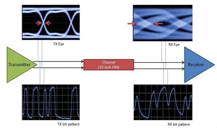
Figure 6. The effect of long rise and fall times on digital signal transmission. Image used courtesy of TI.
At the transmitter side the signal transitions are relatively sharp; however, as the signal reaches the far end of the transmission line, its rise/fall times increase. When several consecutive bits have the same value, the received signal might be able to reach its final value even with the elongated rise/fall times. However, for a bit stream that alternates between 1s and 0s, such as 101010101, the transmitted pulses have a shorter duration and the output doesn’t have enough time to reach its final value. Therefore, whether or not a given transition reaches its final value depends on the bit pattern.
Also, note that the final value for a given transition is the initial value for the next transition. And, hence, the bit pattern affects the initial value of the transitions as well. These undesired effects lead to a data-dependent timing jitter often referred to as intersymbol interference (ISI). The above figure also shows the eye diagram of the transmitted and received signals. An eye diagram is created by superimposing successive waveforms of the signal. Note how the distortion manifests itself with a closed eye diagram. Figure 7 below shows the loss effect on the eye diagram for progressively lossier lines.
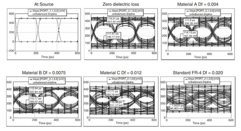
Figure 7. Increasing digital signal distortion for increasingly lossy transmission lines. Image used courtesy of Clyde Coombs.
The chart in the upper-left corner is the transmitted signal. As the Df or loss tangent of the PCB increases from zero to Df=0.020 (corresponding to a typical FR4 board), the line becomes more and more lossy and the eye opening becomes smaller and smaller. The dielectric loss mechanism will be discussed in great detail in a future article. As you can see, the loss has two effects: it attenuates the signal and introduces distortion. The distortion ultimately limits the data rate or calls for equalization.
Loss Consequences in RF Systems
Most RF systems need to process a small signal. An unintentional attenuation of the input signal power is clearly undesired. Another important consequence of having a lossy component in the signal chain, such as a lossy line, is an increase in the noise figure of the system. We discussed in a previous article that when the physical temperature of a passive attenuator with a loss of L is T0=290 K, then its noise factor is F=L (or equivalently, its noise figure in dB is equal to its loss in dB). As an example, assume that a line with a loss of L (in linear terms rather than decibels) precedes an amplifier with noise factor Famp as illustrated in Figure 8.
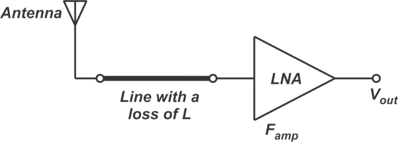
Figure 8. RF receiver system with a lossy transmission line
Applying Friis’ equation, we can find the overall noise factor as:
\[\begin{eqnarray}
F &=& F_1 + \frac{F_2 - 1}{G_1} \\
&=& L + \frac{F_{amp} - 1}{\frac{1}{L}} \\
&=& L \times F_{amp}
\end{eqnarray}\]
Equivalently, we can express the above equation in terms of noise figure values in dB. For example, if the line’s loss is 0.2 dB and the amplifier’s noise figure is 2 dB, the overall noise figure works out to 2.2 dB. Note that the above calculation is based on the assumption that the line and amplifier are perfectly matched, otherwise the analysis can be more complicated. In a future article in this series, we’ll learn about different loss mechanisms in transmission lines.
Featured image used courtesy of Adobe Stock
Related Content