 Facebook
 Google
 GitHub
 Linkedin
Modeling ADCs Using Intermodulation Polynomial and Effective Number of Bits
In this article, we discuss another methodology of how to model ADCs in system simulations, this time by using the effective number of bits and also adjusting our ADC by introducing a 5th order polynomial to the ideal quantizer input.
So far in this series, we've discussed the merits of various ways to model data converters in system simulations, particularly by using a modeling method using the effective number of bits or ENOB.
Now, we'll continue this discussion by adding a new element: adjusting our ADC model directly with a 5th order polynomial added to the ideal quantizer input.
Description of Our New ADC Model
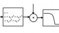
The model presented in our previous article did not result in any distinct spurious frequencies (spurs). Since spurs are an important characteristic of ADC performance, a better model was required.
This is shown in Figure 1.
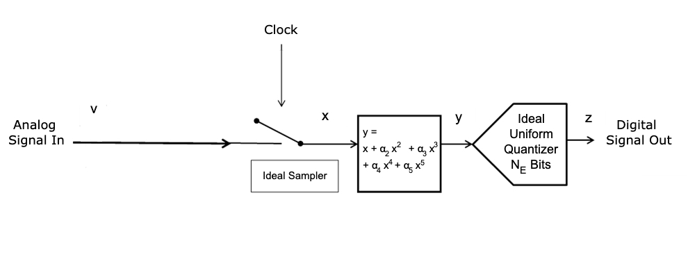
Figure 1.
This adds a 5th order polynomial to the ideal quantizer input.
A two-tone input should be used to determine the parameters αi(fc) and NE(fc); where fc is the center frequency between the tones, as shown in Figure 2 (which you'll recognize as Figure 4 from our first article).
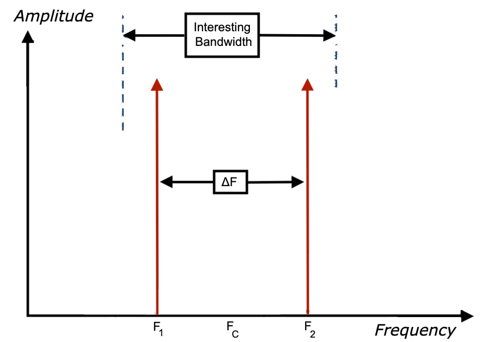
Figure 2.
If any of these parameters are also a function of Δf, the separation between the tones, there is probably a non-linearity with memory in the ADC, and this model would not apply.
As an example, the same two-tone input as shown in Figure 3 (discussed as Figure 3 from our previous article) was used, with NE = 8 bits, α3 = 0.04, and all the other αi = 0. The same Nyquist bandwidth (730.9 MHz) and “interesting bandwidth” (233.7 MHz) as in our previous article exist.
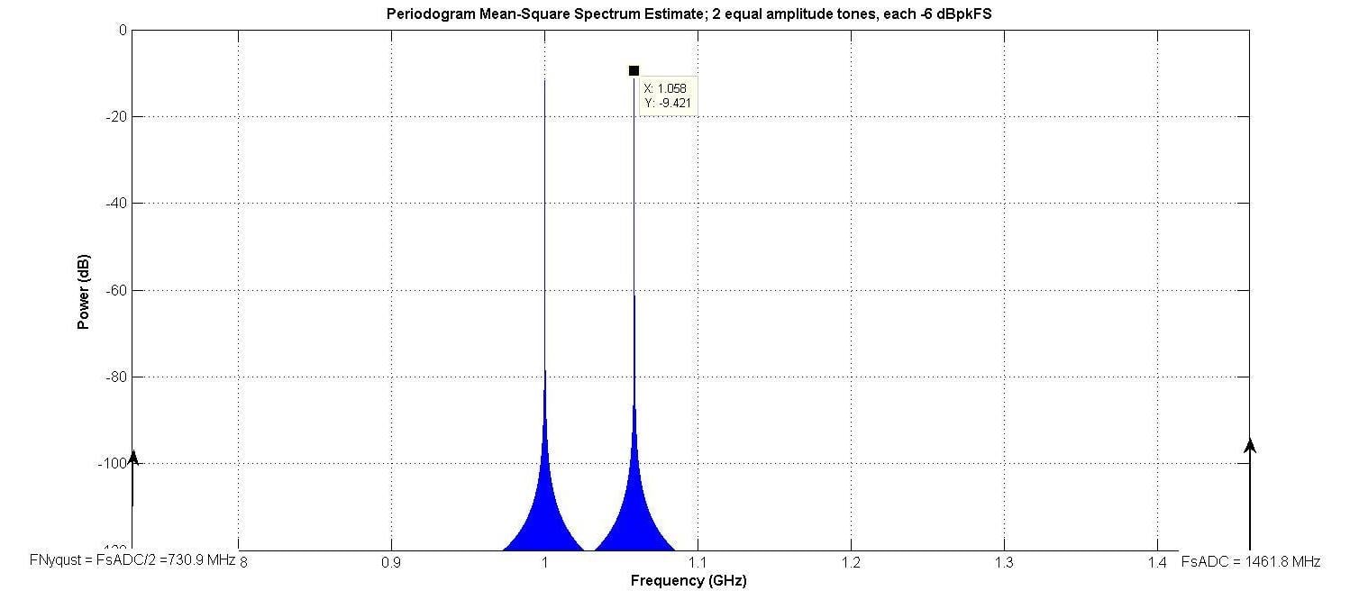
Figure 3.
Figure 4 shows the output with one-tone input, and Figure 5 shows the output with two-tone input.
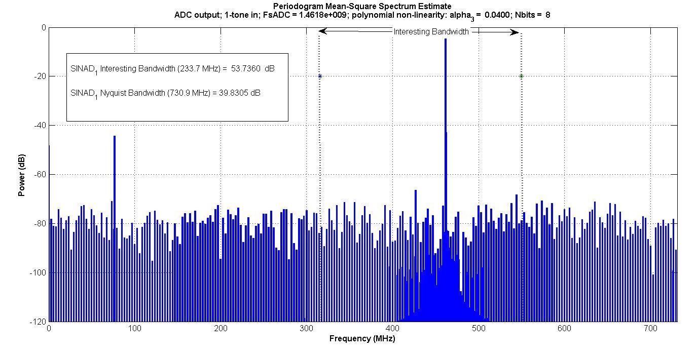
Figure 4.
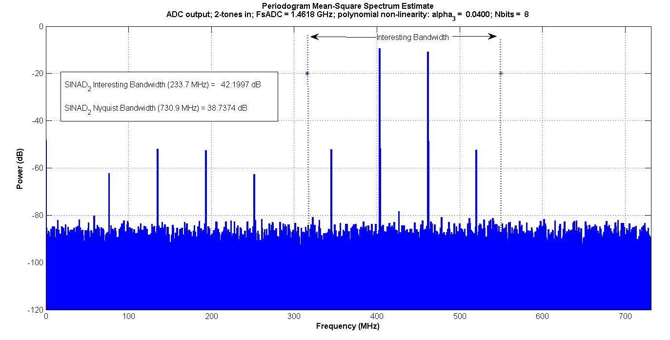
Figure 5.
Intermodulation products appear inside the “interesting bandwidth” for the two-tone input, but not for the one-tone input.
If someone was only measuring inside this “interesting bandwidth”—for instance, if there was a digital bandpass filter which only passed that band—the one-tone test would not capture the intermodulation effect, but the two-tone would.
Figure 6 plots the various SINADs for 5 to 12 input bits. It is apparent that the one-tone input, measured in the “interesting bandwidth”, does not capture the intermodulation effect for more than 7 bits.
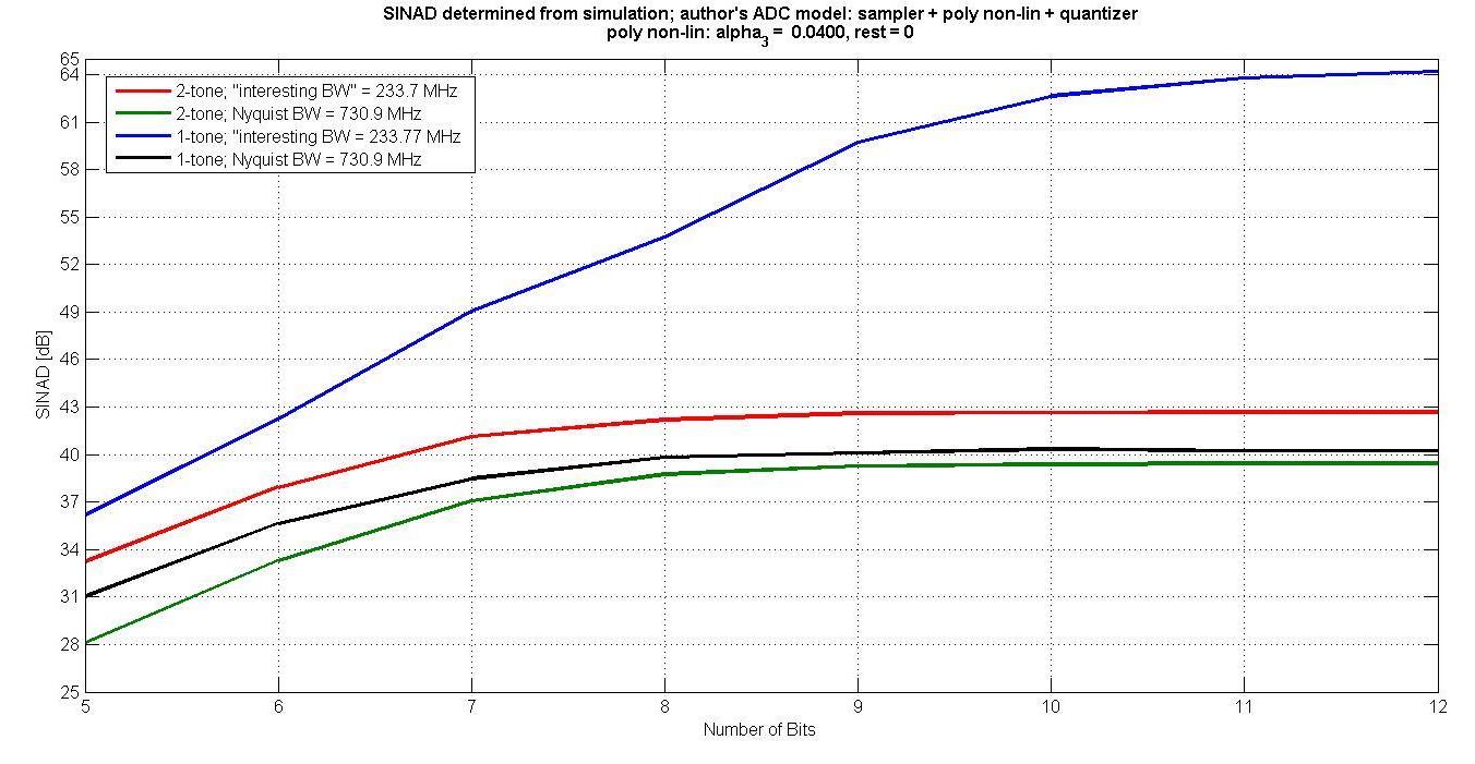
Figure 6.
Also, for more than 7 bits, since the quantization noise decreases as the number of bits increases, but the intermodulation distortion remains the same, the SINAD does not improve with more bits.
Comparison with Manufacturers Model
Dear Reader: You may now be wondering; “So what? These are just some models and their responses to some signals. What's the purpose?”
The purpose should be that two-tone measurements can be made on an ADC, and the parameter values shown in Figure 1 picked to make a best fit to the measured ADC output. This can often be done manually adjusting them until a good fit is obtained. Then, the simplified model can be used in long bit error rate (BER) simulations.
The measurements could be done on an actual device, on a good model for the device, or be obtained from manufacturers' datasheets.
To be a good model, it must closely approximate the actual device; such as a complete SPICE model. Such a complicated model would take too long to run in a BER simulation.
What was available to your author from a manufacturer was what they called a “behavioral” model, which they claimed captured all the important parameters of a particular model ADC. The manufacturer’s model also took into account both internal and external clock jitter. This was used to evaluate the method.
Two-Tone Input
Figure 7 shows the simulation set-up. The two-tone input was generated, and then input to both your author’s and manufacturer’s model. Both were displayed with spectral analysis.
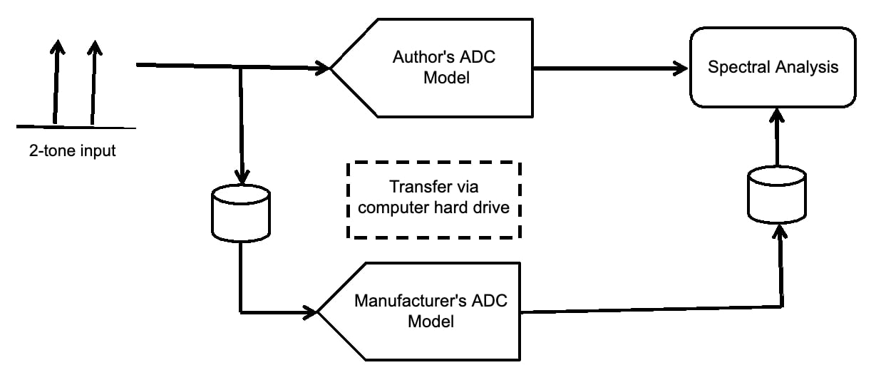
Figure 7.
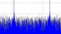
Figure 8 shows the input used. The two tones are between 300 and 350 MHz. The ADC sampling frequency is approximately 250 MHz, so these tones are in the 3rd Nyquist zone.
Since each is at -6.02 dBpeakFS, when they add in phase the voltage will be twice as much, resulting in 0 dBpeakFS.
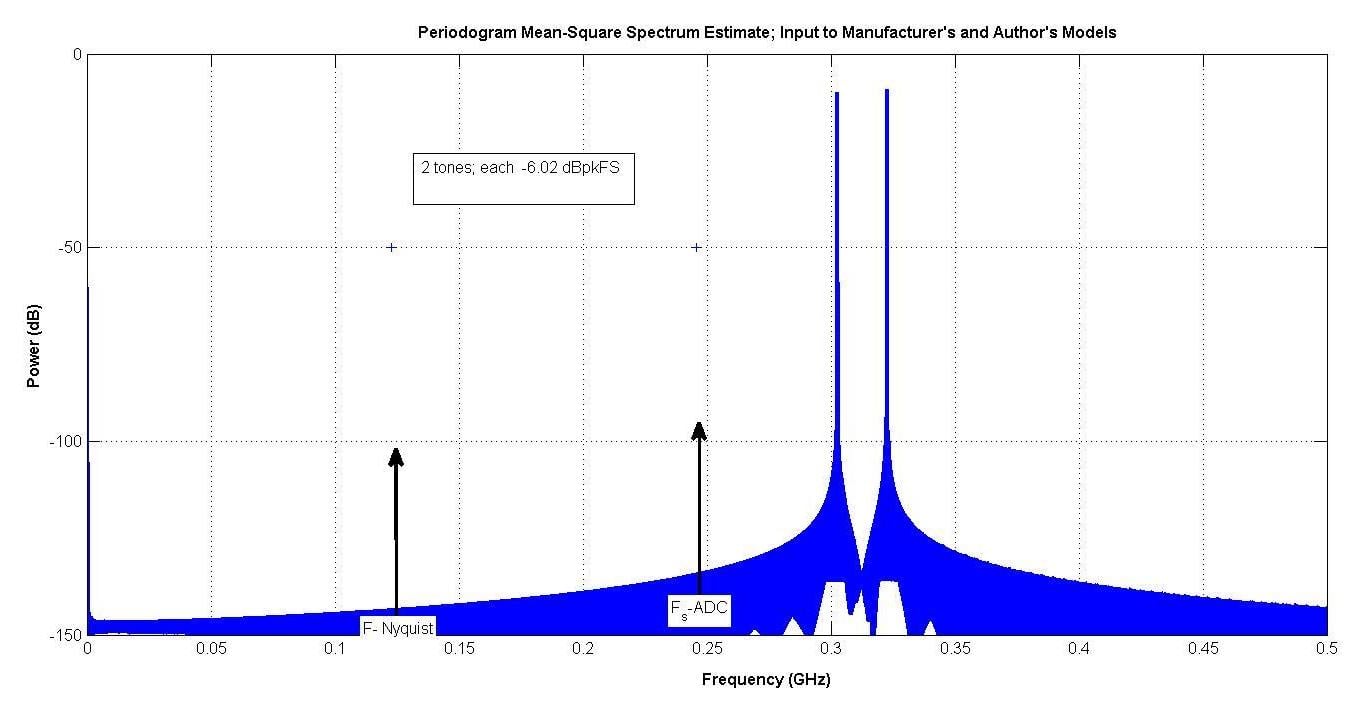
Figure 8.
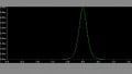
Figure 9 shows the output of the manufacturer’s model, which had a SINAD of 63.74 dB in the “interesting bandwidth” from about 27 to 107 MHz.
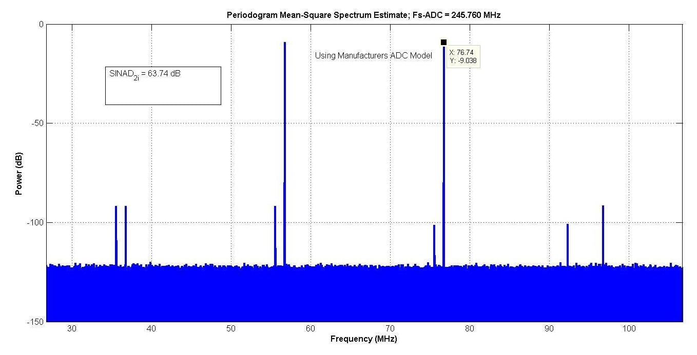
Figure 9.
Figure 10 shows the result after adjusting your author’s model parameters for a match.
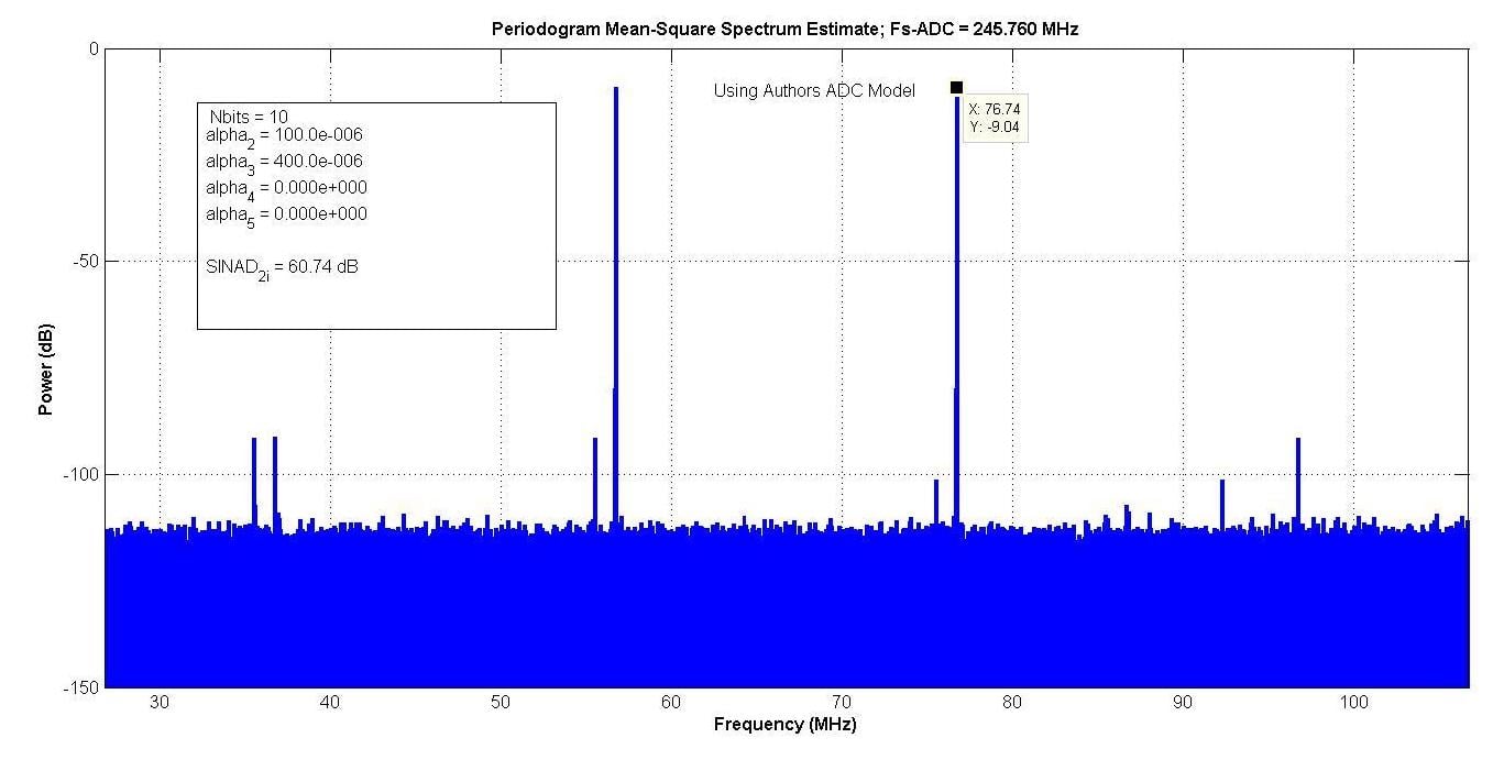
Figure 10.
The polynomial coefficients gave enough degrees of freedom so that an almost exact match could be made to the spurs. NE of 11 bits gave a noise floor 3 dB below the manufacturer’s model, and NE of 10 bits gave it 3 dB above the manufacturer’s model.
Your author decided to use the pessimistic value of 10 bits, which gave a SINAD of 60.74 dB. An improved model would allow up to 6 dB of additive white Gaussian noise to be added, so the higher value of NE could be chosen, and the additional noise added to match the noise floors.
OFDM Waveform Input
The two models can now be compared with a communications waveform as the input.
A commercially available software package comes with an LTE model; which generates an OFDM signal. The model includes a modulator, a frequency-selective Rayleigh fading channel, additive white Gaussian noise, and a demodulator.
It is possible to insert the ADC models in front of the demodulator, and evaluate the spectrum of the ADC output, and the error vector magnitude of the OFDM signal, as is shown in Figure 11.
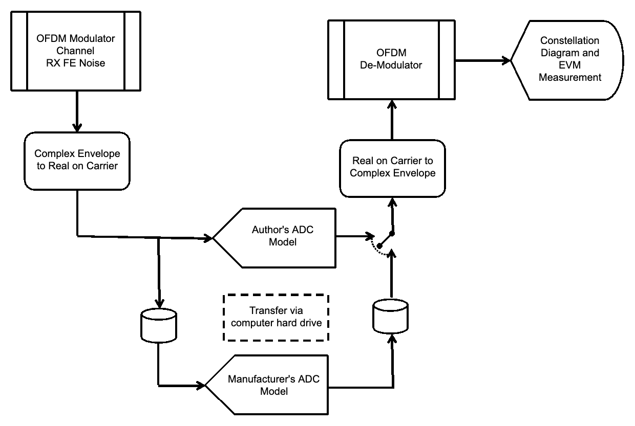
Figure 11.
An OFDM signal which had 64-QAM subcarriers was used. The parameters of your author’s ADC model are the same as used for Figure 10.
The commercially available software package uses complex envelope notation [3] to form its signals. This allows only the modulation information to be tracked sample-to-sample by complex numbers, and the carrier frequency just kept as a known constant. So, the number of samples needed to describe the waveform is greatly reduced.
However, the inputs to the ADC models need to be a real signal on an explicit carrier, to take into account the difference in ADC performance as a function of input frequency. So, the “Complex Envelope to Real on Carrier” and “Real on Carrier to Complex Envelope” transformations [3] needed to be done.
Figure 12 shows the OFDM signal input to both ADC models. It is centered on the same frequency as the two-tones shown in Figure 8.
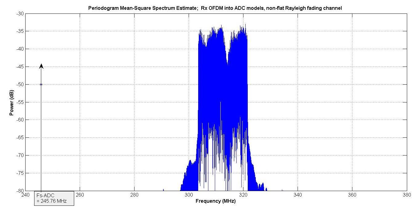
Figure 12.
The dBrmsFS level into both ADC models was -7 dBrmsFS.
Figure 13 shows the spectrum of the manufacturer’s model, and Figure 14 that of your author’s model. Both show spectral regrowth because of the ADCs’ non-linearity. The spectra are very close.
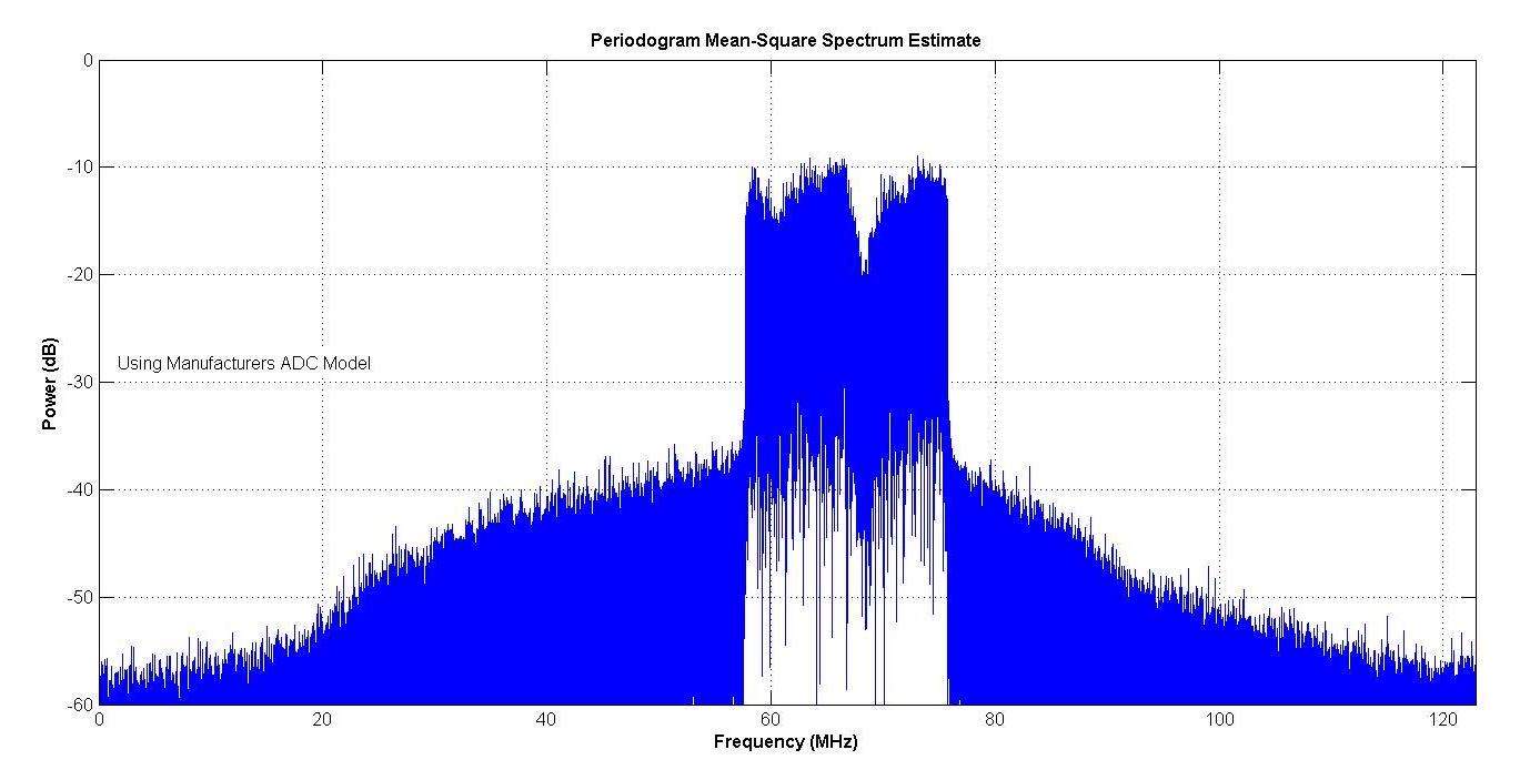
Figure 13.
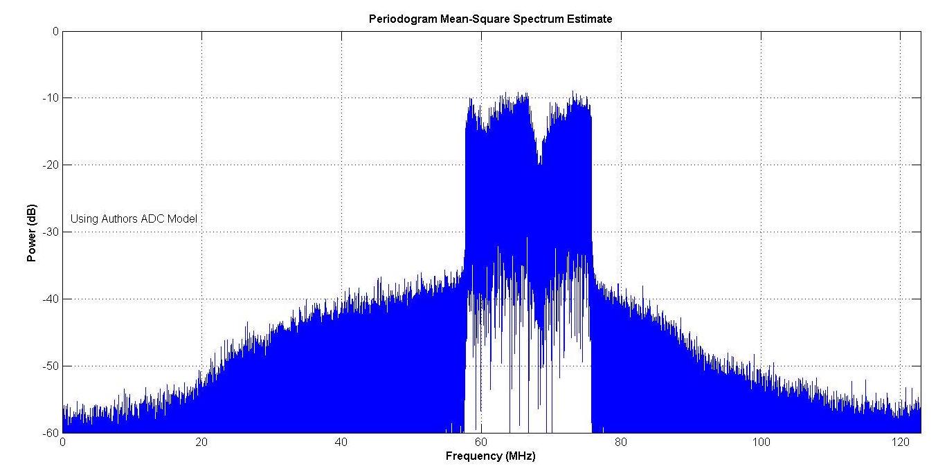
Figure 14.
Figure 15 shows the constellation of the received OFDM for the manufacturer’s model, and Figure 16 shows it for your author’s model.
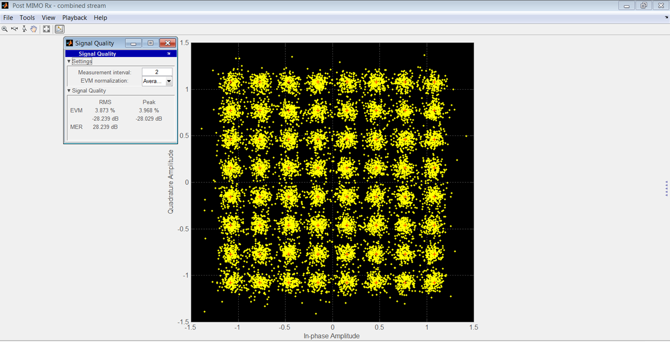
Figure 15.
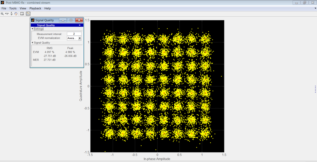
Figure 16.
A comparison of rms and peak EVMs is in Table 3. The SNR was 90 dB for these results.
Table 3.

Over a range of -7 to -47 dBrmsFS, the rms difference between EVMs of the two models was 3.46 dB.
Overall, your author’s model gives very similar results as the manufacturer’s, for a fairly simple set of parameters. No information on the manufacturer’s model was available, but it may be similar to your author’s.
In any case, the simulations ran faster when using your author’s model, because it was not necessary to transfer data between simulation software. So, your author’s model was used in the bit error rate (BER) simulation shown in Figure 17.
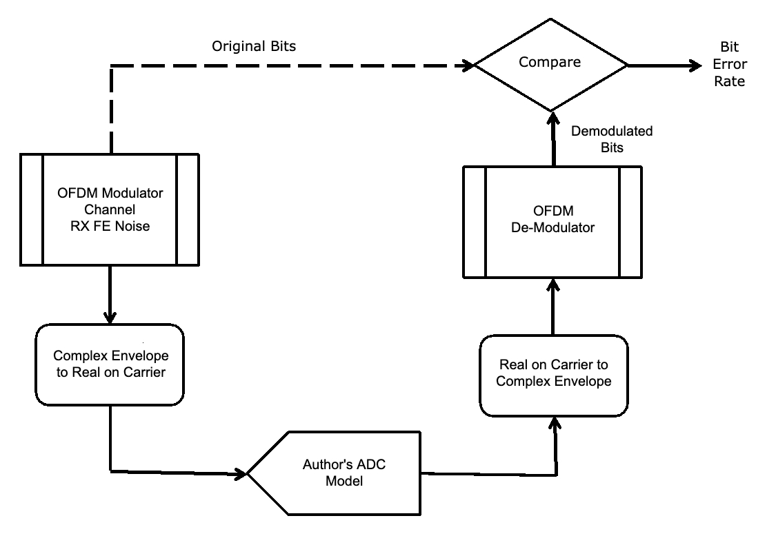
Figure 17.
One important parameter when designing a system with an ADC is the optimum level to place the signal relative to ADC full scale.
Too low a level results in the signal being too small relative to the noise and distortion.
Too high a level results in excessive clipping, which also distorts the signal. Usually, a level which allows some clipping is optimum.
The BER for three different SNRs and signal levels from -41 to -7 dBrmsFS is shown in Figure 18.
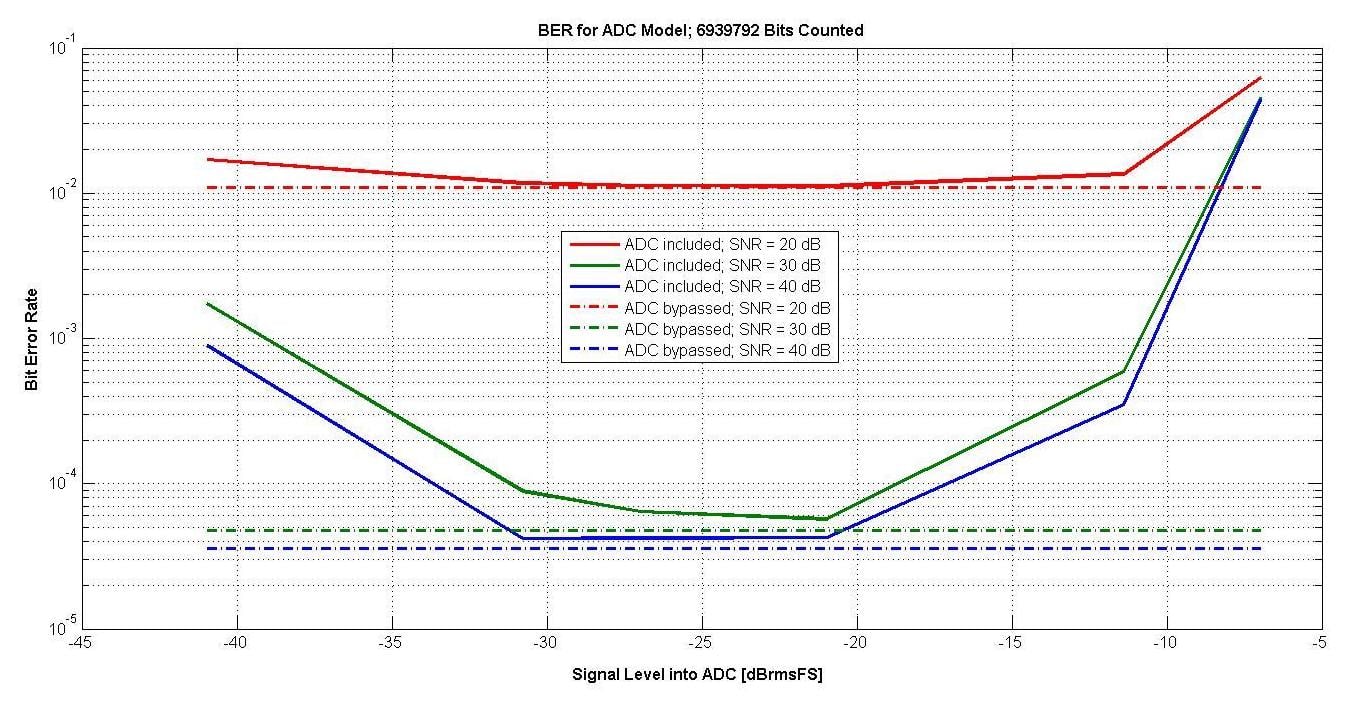
Figure 18.
Also shown with the dashed lines is the BER when the ADC model is bypassed. With the ADC, there is about a 10 dB range which is optimum, and an automatic gain control should keep the signal in this range.
In the next article, we'll finish up this series by concluding with some thoughts on a better model to use and also talk a bit about models for DACs. Please share your thoughts on this series in the comments below.


The questions might arise; “Why add the extra complexity of the polynomial to the model? Why not just include distortion products as part of the Effective Number of Bits like the previous article in this series?”
The answer is that the A/D converter, in this application is being used as an RF (Radio Frequency) Device. For RF devices, we do not apply a test signal, measure distortion products, and include those products as part of the Noise Figure. Depending on the input signals, distortion products might or might not fall within the desired signal bandwidth. Distortion products for RF devices are usually taken into account by the third order intercept. The third order intercept could be determined by the polynomial in this model.
This is why the model with a polynomial to take into account non-linear distortion products, together with a “Noise Effective Number of Bits” to take into account quantization noise, clock jitter, and other noise-like phenomena is better.