 Facebook
 Google
 GitHub
 Linkedin
PCB Layout for a Photovoltaic Power Supply for Microcontroller Circuits
This article discusses the PCB layout for a power-supply circuit that generates a regulated 3.3 V rail from a small solar cell.
This article discusses the PCB layout for a power-supply circuit that generates a regulated 3.3 V rail from a small solar cell.
If you’ve read my previous article, Schematic Design for a Solar-Powered Charge-Pump Power Supply, you know that my goal with this project was to create a very simple, very compact circuit that could power a microcontroller-based embedded system. The circuit was intended to be active only during the hours of abundant illumination, because the design does not include a capacitor or battery for storing surplus energy.
In this article, I'll go over the PCB layout for the circuit from my power supply schematic.
Related Information
Before continuing, consider reading these related articles for some background information:
- Boosting and Inverting without Inductors: Charge-Pump Power Supplies
- The Circuit Designer’s Guide to Photovoltaic Cells for Solar-Powered Devices
- Selecting and Implementing Photovoltaic Cells for Solar-Powered Devices
PCB Layout for a Photovoltaic Power Supply
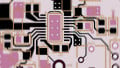
The following images show the layout for the top and bottom of the PCB. All the components and most of the traces and copper pours are on the top; the bottom is primarily a ground plane.


PCB Dimensions
The microcontroller is an EFM8 Sleepy Bee from Silicon Labs, and the (relatively) large connector on the left provides a direct connection to the SiLabs USB debug adapter. This connector consumes quite a bit of PCB real estate and makes the overall design look larger than it really is.
The following image shows the dimensions of the PCB (in inches). The shorter horizontal dimension is my attempt to estimate how small the board could be if the debug connector were removed (and the other components rearranged).

So my guess is that a two-layer board with all the components on one side could be less than 1.5 square inches. I’d say that’s pretty good, especially considering that we’re talking about a two-layer PCB.
Furthermore, I don’t think that I’m losing any performance by using two layers instead of four, because the bottom side is almost a solid ground plane and there is plenty of room on the top for wide power traces and generously sized ground connections (and also because the microcontroller will be operating at very low frequency).
Small, But It Could Be Smaller
Here are some other ways in which the size of this board could be reduced:
- I chose larger passive components (0805 and 1206) because they’re easier to assemble. If you plan to have the board assembled professionally, you could consider using 0603s or even 0402s (you might be able to find acceptable 2.2 µF caps in an 0402 package, but you could definitely go with 0402 for the 0.1 µF capacitor and the resistors).
- I chose a larger package for the microcontroller as well; it’s a 9 mm × 9 mm QFP32. The 32-pin no-leads package is significantly smaller (5 mm × 5 mm), and there is also a 24-pin no-leads package that is even smaller (4 mm × 4 mm). It seems to me that most applications built around this power supply wouldn’t need more than a handful of I/O pins, so the 24-pin package is probably the best option. I used a 32-pin device only because this microcontroller doesn’t come in any other leaded (i.e., non-no-leads) package.
- I included a high-precision 32.768 kHz crystal for real-time clock applications; it’s about the size of an 0805 component. The microcontroller has an internal low-power oscillator with terrible accuracy (±10%), so if you have no need for precision timing you could omit the crystal.
- The charge-pump switching regulator currently has four 2.2 µF output capacitors, but only one is required.
- The LED and its accompanying resistor are for debugging only; they could be omitted in the final design.
- You might be thinking that you could eliminate all the circuitry associated with the debug power supply (a switch, an LDO, and two capacitors). I wouldn’t recommend that, because the solar-powered supply is not a convenient power source for firmware development and testing.
The Two-Sided Option
The last item on the how-to-make-it-smaller list is to have components on the top and bottom side of the board. As I was writing this article I started to wonder if the entire circuit could fit in an area corresponding to the size of the solar cell, such that you could design a board with only the solar cell on the top and everything else on the bottom. I decided to eliminate some unnecessary components from the schematic and then give this idea a try, and here is what I found (dimensions are in inches):


This is a rough approximation, but nonetheless, you can see that we’re pretty close to the goal of cramming all the circuitry into the PCB real estate occupied by the solar cell.
To create this component placement I eliminated three of the four output capacitors, the crystal, the LED, and the LED’s resistor. I also switched the microcontroller package to a QFN24. The passive components are still 1206 and 0805, but these larger packages compensate for the fact that you would need some means of connecting the microcontroller to the debug adapter. There certainly wouldn’t be much space for routing, but I don’t think that’s a serious impediment if you can use a four-layer board (and there is also plenty of empty space on the top side underneath the solar cell).
Conclusion
We’ve discussed the PCB layout for a solar-powered microcontroller board that I recently designed, and we also looked at an example of a more space-optimized implementation in which the size of the PCB approaches the size of the solar cell. If you have any experience with space-constrained design for low-power embedded devices, feel free to share your thoughts in a comment.
Related Content


Why is the SW1 still present in the compact design when there is no apparent debug interface to provide the power being switched? I realize it can still function as an on/off for the uC, but in this design, without a radio module that you might be transmitting cruft over, that seems less necessary.
BOM (and board size) could be reduced by making an intermediate debug adapter that incorporates the special debug header and the regulator (which needn’t be on the deployed device) - the necessary IO for that could be brought out to pads along one edge of the PCB so that they could be solder bridged or pogo-pinned to the debug interface PCB. An SO type IC debug clip with slight modifications can be used to connect the debug PCB to the target board by biting the PCB edge.
If your uC has an unused ADC, you might consider routing the output of the charge pump to that, possibly via a solder bridge or unpopulated 0R (or even a current-limiting value), so that the uC could monitor the voltage (say, while being debugged and powered by the debug interface).
Nice and good article. It is very useful for me to learn and understand easily. Thanks for sharing your valuable information and time. Please keep updating IOT online training hyderabad