 Facebook
 Google
 GitHub
 Linkedin
Understanding the Successive Approximation Register ADC
One of the most common analog-to-digital converters used in applications requiring a sampling rate under 10 MSPS is the Successive Approximation Register ADC. This ADC is ideal for applications requiring a resolution between 8-16 bits.
The Successive Approximation Register ADC is a must-know.
One of the most common analog-to-digital converters used in applications requiring a sampling rate under 10 MSPS is the Successive Approximation Register ADC. This ADC is ideal for applications requiring a resolution between 8-16 bits. For more information on resolution and sampling rates, please refer to the first in this series of articles: Deciphering Resolution and Sampling Rate. The SAR ADC is one of the most intuitive analog-to-digital converters to understand and once we know how this type of ADC works, it becomes apparent where its strengths and weaknesses lie.
Basic Operation of the SAR ADC
The basic successive approximation register analog-to-digital converter is shown in the schematic below:
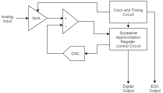
The SAR ADC does the following things for each sample:
- The analog signal is sampled and held.
- For each bit, the SAR logic outputs a binary code to the DAC that is dependent on the current bit under scrutiny and the previous bits already approximated. The comparator is used to determine the state of the current bit.
- Once all bits have been approximated, the digital approximation is output at the end of the conversion (EOC).
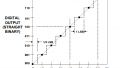
The SAR operation is best explained as a binary search algorithm. Consider the code shown below. In this code, the current bit under scrutiny is set to 1. The resultant binary code from this is output to the DAC. This is compared to the analog input. If the result of the DAC output subtracted from the analog input is less than 0 the bit under scrutiny is set to 0.
%8−bit digital output is all zeros
digital output = zeros(1,8);
%Normalised to one for example
reference voltage = 1;
for i=1:8
 %current output bit set to 1:
 digital output(i)=1;
 compare threshold = 0;
 %Output digital output in current form to DAC:
 for j=1:i
  compare threshold = compare threshold+digital output(j)*reference voltage/(2ˆj);
 end
 %Comparator compares analog input to DAC output:
 if (input voltage−compare threshold<0)
  digital output(i)= 0;
 end
end
If we consider the example of an analog input value of 0.425 V and a voltage reference of 1 V, we can approximate the output of an 8 bit ADC as follows:
- Set first bit of 8 bit output to 1 so output to DAC is 0.5
- 0.5 subtracted from 0.425 is less than 0, so set the first bit of output to 0
- Set second bit of 8 bit output to 1, so output to DAC is 0.25
- 0.25 subtracted from 0.425 is greater than 0, so second bit of output is 1
- Set third bit of 8 bit output to 1, so output to DAC is 0.375
- 0.375 subtracted from 0.425 is greater than 0, so third bit of output is 1
This process is repeated for all 8 bits until the output is determined to be:
01101100
It becomes apparent from this process that an N-bit SAR ADC must require N clock periods to successfully approximate the output. As a result of this, although these ADCs are low power and require very little space, they are not suitable for high speed, high resolution applications. Because these ADCs require very little space, they are often found as a peripheral inside microcontrollers or in an extremely small package.
Perhaps slightly less intuitive is the fact that power dissipation scales with sampling rate. As a result of this, these ADCs are ideal for use in low power applications where the ADC is required to take samples infrequently.
One thing to note in this architecture is the lack of a pipeline and the latency associated with this. As a result, the SAR ADC is suited to multiplexed applications.
The two features of the ADC that define the overall characteristics of the ADC are not surprisingly, the DAC and the Comparator.
The Capacitive DAC
A capacitive DAC contains N capacitors for an N-bit resolution with the addition of a second least significant bit capacitor. An example of a capacitive DAC is shown below:
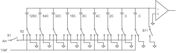
During acquisition, the common terminal is connected to ground by closing S11 and the analog input (Ain) is charging and discharging the capacitors. The hold mode occurs if the input is disconnected by opening S1. S11 is then opened driving the common terminal to -Ain. If S2 is then connected to Vref, a voltage equal to Vref/2 is added to -Ain. The decision about the most significant bit is determined following this.
The maximum settling time of a capacitive DAC is determined by the settling time of the most significant bit. This is due to the fact that the largest change in the DACs output occurs due to this most significant bit.
You may be forgiven for thinking that a 16-bit SAR ADC would take twice as long to produce the output as an 8-bit SAR ADC because of the fact that there are twice as many output bits. In reality, the settling time of the internal DAC in the 16-bit SAR ADC would take far longer than the settling time of the 8-bit version. As a result of this, the sampling rate of high resolution SAR ADCs is reduced significantly when compared to low resolution versions.
The linearity of the overall ADC is dependent on the linearity of the internal DAC. As a result of this, the ADC resolution is, not surprisingly, limited by the resolution of the internal DAC.
The Comparator
The comparator is required to be both accurate and fast. As with the DAC, it should come as no surprise that the comparator must have a resolution at least as good as the SAR ADC. The noise associated with the comparator must be less than the least significant bit of the SAR ADC.
Summary
Strengths of the SAR ADC
- Low power consumption
- Physically Small
Weaknesses of the SAR ADC
- Low sampling rates for high resolutions
- Limited resolution due to limits of DAC and Comparator
- Size increases with number of bits
Applications of the SAR ADC
Ideal for multichannel data acquisition systems with sampling frequencies under 10 MHz and resolutions between 8-16 bits.
Next Article in Series: Understanding the Delta-Sigma ADC


Step 4 says: 0.25 subtracted from 0.425 is greater than 1, so second bit of output is 1.
0.425 - 0.25 = 0.175 !> 1
What’s it supposed to say, that it’s greater than zero?