 Facebook
 Google
 GitHub
 Linkedin
Universal Logic Gates
NAND and NOR gates are widely known to be universal logic gates, meaning that any other logic gate be made from NAND or NOR gates. This article discusses other universal logic gates.
Introduction
A universal logic gate is a logic gate that can be used to construct all other logic gates. There are many articles about how NAND and NOR are universal gates, but many of these articles omit other gates that are also universal gates. This article covers two input logic gates, demonstrates that the NAND gate is a universal gate, and demonstrates how other gates are universal gates that can be used to construct any logic gate.
Two Input Logic Gates
For 2 logical inputs, there are 16 possible logic gates. Table 1 defines the 16 logic gates, shows logical symbol, behavior in symbolic logic, provides name, notes.
People are most familiar with the ones that are named: NAND, NOR, AND, OR, XOR. Table 1 includes these, as well as AND and OR gates with either input negated, logic 0 and logic 1(which aren't really logic gates), and some gates that aren't really binary.
| Output when AB is | ||||||||
| Gate # | 00 | 01 | 10 | 11 | Symbolic Logical Description | Symbol | Name/Description | Note |
| 0 | 0 | 0 | 0 | 0 | 0 |  |
Always zero | Not really a gate |
| 1 | 0 | 0 | 0 | 1 | A & B |  |
AND | |
| 2 | 0 | 0 | 1 | 0 | A & ~B |  |
A and Not B | Universal |
| 3 | 0 | 0 | 1 | 1 | A |  |
A | Not BInary |
| 4 | 0 | 1 | 0 | 0 | ~A & B |  |
B and Not A | Universal |
| 5 | 0 | 1 | 0 | 1 | B |  |
B | Not Binary |
| 6 | 0 | 1 | 1 | 0 | (A & ~B) | (~A & B) |  |
XOR | Also Not Equals Function |
| 7 | 0 | 1 | 1 | 1 | A | B |  |
OR | |
| 8 | 1 | 0 | 0 | 0 | ~(A | B) |  |
NOR | Universal |
| 9 | 1 | 0 | 0 | 1 | (A & B) | (~A & ~B) |  |
XNOR | Also Equals Function |
| 10 | 1 | 0 | 1 | 0 | ~B |  |
Not B | Not Binary |
| 11 | 1 | 0 | 1 | 1 | A | ~B |  |
A or Not B | Universal |
| 12 | 1 | 1 | 0 | 0 | ~A |  |
Not A | Not Binary |
| 13 | 1 | 1 | 0 | 1 | ~A | B |  |
B or Not A | Unversal |
| 14 | 1 | 1 | 1 | 0 | ~(A & B) |  |
NAND | Universal |
| 15 | 1 | 1 | 1 | 1 | 1 |  |
Always 1 | Not really a gate |
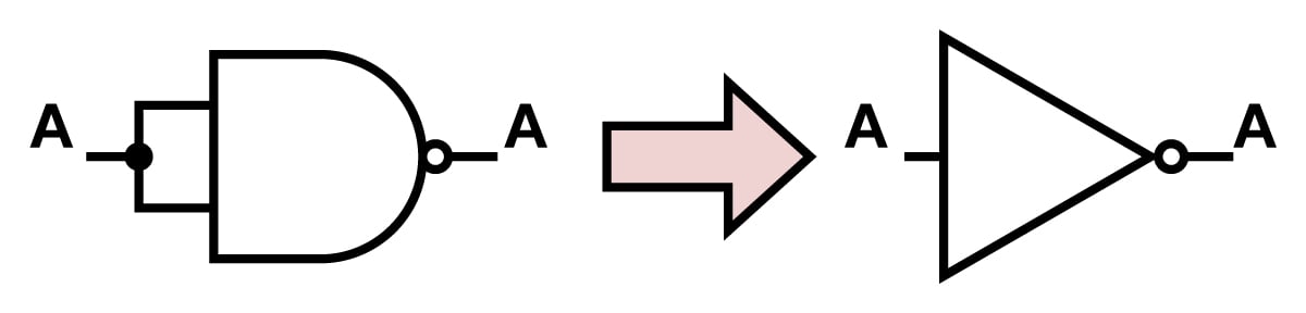
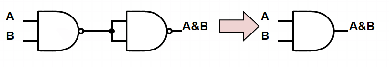
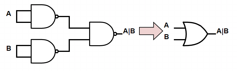
NAND Gate is a Universal Gate
NAND gates can be connected to form any other logic gates. Figures 1,2,3 show how NAND gates can be connected to form INVERTER, AND, and OR gates. These gates can be combined to form the other logic gates according to the symbolic logic definitions in table 1.
Other Universal Gates
Gates 2,4,11, and 13 are universal gates. To prove this, we demonstrate building NAND gates with these gates. Gates 7 and 8 are the same gate but with different inputs inverted. Gates 9 and 10 are the same gate but with different inputs inverted. Proving that gates 2 and 11 are universal is enough to prove that gate 4 and 13 are universal as well.
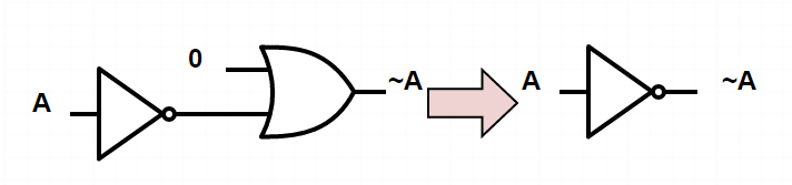
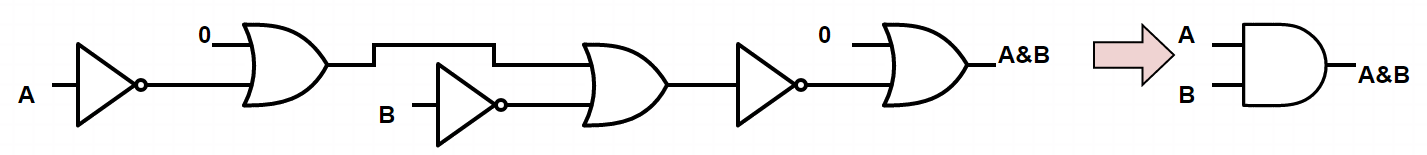
Gate 11: A | ~B
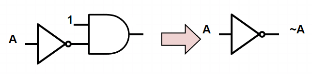
Figures 4 and 5 show show gate 11 can be combined to create INVERTER and AND gates. INVERTER and AND gates can be connected in series to construct a NAND gate. Because gate 11 can be used to construct a NAND gate, and a NAND gate is a universal gate, gate 11 is a universal gate. Since gates 11 and 13 are mirrors of each other, gate 13 is also a universal gate.
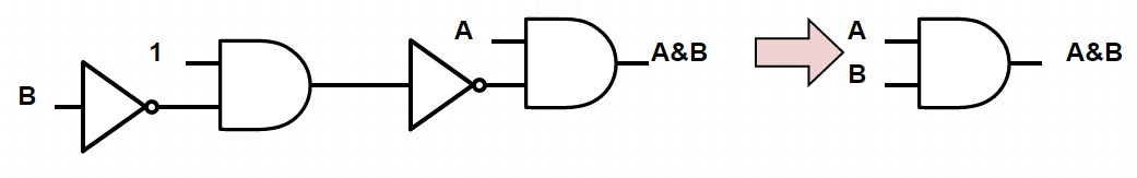
Gate 2: A & ~B
Figures 6 and 7 show show gate 2 can be combined to create INVERTER and AND gates. INVERTER and AND gates can be connected in series to construct a NAND gate. Because gate 2 can be used to construct a NAND gate, and a NAND gate is a universal gate, gate 2 is a universal gate. Since gates 2 and 4 are mirrors of each other, gate 4 is also a universal gate.
Conclusion
This article has discussed logic gates, universal gates, demonstrated that the NAND gate is a universal gate, and proven that four additional universal logic gates exist. This is an interesting academic exercise. In practice, the author would recommend sticking to using NAND gates as universal gates because they are so cheap and small to construct, or if doing board level design using chips with the actual gates that are wanted and not using universal gates.


loved the nixie tubes pic!
It’s good if we remember the universal gates. But, if we don’t remember what they are exactly then it is not all going to be easy to realized .
Is there any trick that helps us to know whether the given gate is a universal gate?!!??