 Facebook
 Google
 GitHub
 Linkedin
Combinational Logic Circuit Design and Simulation Using Gates
Gate-level implementation of logic functions is limited by the gate fan-in. This article examines logic factoring, grouping, and level increases to implement logic functions with limited input gates.
Learn how to utilize combinational logic functions and simplify combinational logic circuits! In order to understand the challenges associated with these processes, let's start by establishing a real-world example to demonstrate the concept.
Why Are the Number of Gate Inputs Limited?
Imagine we are designing a logic system to initiate an alarm signal (S) if any of six emergency exits are opened. The output from the alarm system is normally high (logic 1) and will initiate the alarm by going low (logic 0). The door sensors (labeled a through f) each output a logic 0 when they are closed and output a logic 1 when they are opened.
We can easily represent this logic function as:
$$S = \overline{a + b + c + d + e + f }$$
Implementing this in a single-level logic function with a six-input NOR gate would be straightforward. Theoretically, we could extend the design of the two-input NOR gate shown in Figure 1 to support the required six inputs.

Figure 1. CMOS 2-input NOR gate
The six parallel NMOS transistors are not necessarily a problem. However, the series stack of six PMOS transistors is not typically feasible because of the limited supply voltage (Vdd). Because of this, basic logic gates are typically limited to some maximum number of inputs (four is common). The number of inputs to the logic gate is referred to as the fan-in.
Grouping to Design Using Gates with Limited Inputs
For our alarm system problem, we can group and factor inputs to allow us to implement the combination circuit design using gates with a maximum of three inputs each. This is a more reasonable fan-in for a low voltage logic process.
One possible factorization that achieves this is:
$$S = \overline{(a + b + c) + (d + e + f)}$$
The result here is a two-level logic system, as shown in Figure 2, in which all three gates have a maximum of three inputs.

Figure 2. Gate-level logic for alarm system limited to maximum 3-input gates
Implementing a Complex Logic Function with Limited Fan-in
For more complex logic functions, a process of factoring, regrouping, and increasing the number of logic levels can be repeated as needed until all gates meet the maximum fan-in limit of the logic technology being used.
Let’s take a closer look at a more complicated logic function represented by the Karnaugh map of Figure 3.

Figure 3. A Karnaugh map
We can derive the logic equation from the Karnaugh map by grouping the neighboring 1’s terms. First, we can group the top row as shown in Figure 4.
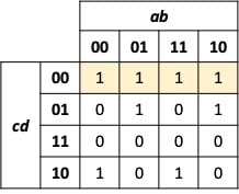
Figure 4. Term grouping of Karnaugh map
For this top row, we can derive the partial logic function as:
$$f_1 = \overline{c}\overline{d}$$
Similarly, we can create four additional groupings of neighboring 1’s terms as illustrated in Figure 5.

Figure 5. Additional term grouping of the Karnaugh map
For these four groupings, we can derive the remaining terms for the logic function:
$$f_2 = \overline{a}\overline{b}\overline{d} + \overline{a}b\overline{c} + ab\overline{d} + a\overline{b}\overline{c}$$
Combing f1 and f2, we get:
$$f = \overline{c}\overline{d} + \overline{a}\overline{b}\overline{d} + \overline{a}b\overline{c} + ab\overline{d} + a\overline{b}\overline{c}$$
To implement this logic function as a two-level system would require a five-input NOR gate to sum all of the terms. If we assume that we are again limited to at most three-input gates, we will need to factor, group terms, and increase the number of levels.
We can regroup as follows:
$$f = \overline{c}\overline{d} + (\overline{a}b\overline{c} + a\overline{b}\overline{c}) + (ab\overline{d} + \overline{a}\overline{b}\overline{d})$$
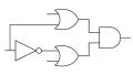
We could implement this function with only three-input gates, but let's factor out some common terms. This might be done if having shorter signal paths for c and d was desirable in the circuit, for example.
$$f = \overline{c}\overline{d} + \overline{c}(\overline{a}b + a\overline{b}) + \overline{d}(ab + \overline{a}\overline{b})$$
This function can now be implemented with gates with a maximum fan-in of three. The resulting gate-level logic function is shown below in Figure 6.

Figure 6. Gate-level logic for logic function limited to maximum three-input gates
Gate-level Logic Synthesis
Most often in modern digital integrated circuit design, the conversion of logic functions into a gate-level implementation will be performed by a gate-level logic synthesis process. A digital standard cell logic library will have a suite of logic gates for use in creating the desired function in hardware. The electronic design automation (EDA) software will convert the logic function described in a higher-level language like Verilog into a physical, gate-level implementation using only the gates available in the library.
The fan-in of the gates available in the standard cell library will be limited by the target semiconductor process and the operating conditions for voltage and temperature. Therefore, the EDA software must perform the factoring, regrouping, and increasing of the number of logic levels as described in this article.
Gate-level Logic Simulation
In an ideal logic simulation, the output changes instantaneously with any change on the inputs. In a real system, there is a “propagation delay” as the input voltage change propagates through the transistors in the circuit to cause a change in the output voltage. The output loads and the rise and fall times of the input and output signals also affect the total circuit signal propagation characteristics.
Timing Diagrams
Let’s look at the simple example of an inverter timing diagram as shown below in Figure 7. As the input, x, changes logic state, the output changes after a delay.
In this example, the falling output propagation delay, df, is shorter and has a steeper slope than the rising output delay, dr. The delays are measured at the 50% level between the two logic levels. This type of asymmetric response would occur in a CMOS inverter in which the NMOS and PMOS transistors were the same size. The higher drive current of the NMOS transistor would pull the output down more quickly than the PMOS transistor could pull the output up.

Figure 7. The timing diagram for an inverter
Timing diagrams can also be used to evaluate logic circuits with multiple inputs and gates. In the example circuit of Figure 8, the changes at input a propagate through the first NAND gate to output x with input-to-output propagation delay d.

Figure 8. The timing diagram for a multi-level logic circuit
The change in the value of x then propagates through the second NAND gate to output y with an additional propagation delay d. Therefore, the total propogation delay from a to y is 2d.
This article provides an introduction to simplifying combinational logic circuits to support limited fan-in gates. In addition, gate-level logic simulation and timing diagrams have been explored briefly.
With this background, in our next article, we'll examine hazards in combinational logic circuits that can cause logic errors if not handled properly.


Great article and so well illustrated. May I ask what tool you used to draw the diagrams and the circuits?
Very informative! I like how it highlights the foundation for optimisation procedures in EDA synthesis tools.