 Facebook
 Google
 GitHub
 Linkedin
Use the Xilinx System Generator to Implement a Simple DDS
In this article, we’ll discuss implementing a simple direct digital synthesizer (DDS) using the Xilinx System Generator.
In this article, we’ll discuss implementing a simple direct digital synthesizer (DDS) using the Xilinx System Generator.
System Generator is a powerful tool that integrates Xilinx FPGA design process with MATLAB’s Simulink which uses a high-level description to easily realize a complex system. We first design the system and verify its functionality in the Simulink environment. The graphical high-level description of Simulink significantly facilitates modeling, simulating, and analyzing the design. Then, we can generate the VHDL description of the design and add it to our project in the Xilinx ISE software.
In this article, we’ll discuss implementing a simple direct digital synthesizer (DDS) using the Xilinx System Generator.
Starting the System Generator
Before launching the System Generator, you should note two points:
- Make sure that your System Generator version is compatible with the MATLAB version that you’re going to use.
- Associate the MATLAB software with your System Generator.
In this article, I will use ISE 14.7 with MATLAB 2013a. The recommended way to start the System Generator is by choosing "Xilinx Design Tools\ISE Design Suite 14.7\System Generator\Sysgen Generator" from “All Programs” menu of Windows. This will open the “Simulink Library Browser” which is shown in Figure 1.
Figure 1
As shown in the figure, the following three Xilinx categories are added to the list of the libraries:
- Xilinx Blockset
- Xilinx Reference Blockset
- Xilinx XtremeDSP Kit
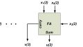
In this article, we will use the blocks provided in the “Xilinx Blockset” to implement a simple DDS as shown in Figure 2.
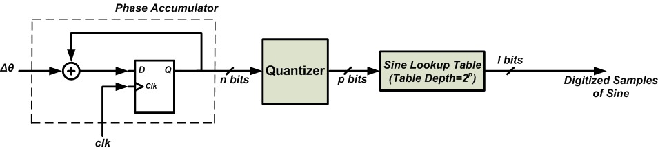
Figure 2
Creating a System Generator Model for the DDS
To create a new Simulink model, choose File\New\Model. This will open the following blank window which allows us to describe the block diagram of Figure 2.
Figure 3
In the rest of the article, we will add the required building blocks and review the important settings in each block’s dialog box. For more information about the configurable parameters of the different blocks, please refer to this Xilinx document.
AddSub Block
The first block that we need is an adder. We can use the “AddSub” block that can be found in the “Xilinx Blockset\math” category. Figure 4 below shows the symbol and the “Basic” tab of the configurable parameters for this block.
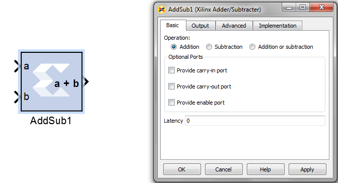
Figure 4
The block has two inputs (a and b) and one output which gives a+b. We will leave the parameters of the “Basic” tab as they are. The settings of the “Output” tab is shown in Figure 5. This tab sets the parameters of the output. To have a 16-bit accumulator, we choose the “User Defined” option which allows us to set the “Number of bits” to 16 and the “Binary point” to zero. This means that the output is a 16-bit integer. For the DDS of Figure 2, we don’t need to define a fractional output but, if we had set the “Number of bits” to 16 and the “Binary point” to 14, 14 bits out of the total 16 bits of the output will be considered to the right of the binary point. To read more about the fixed-point representation in general, refer to this article.
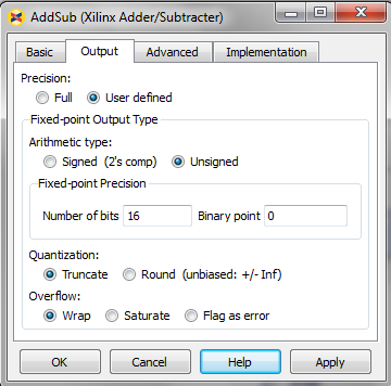
Figure 5
“Arithmetic type” and “Overflow” are two other parameters that are important to us. The “Arithmetic type” should be unsigned because the output of the accumulator is interpreted as an unsigned number. The “Overflow” should be set to “Wrap” because the accumulator should roll over when reaching its maximum.
Figure 6 shows the “Implementation” tab of the block. In this page, you can choose to implement the adder using either the Fabric or the DSP48 slices. For a discussion about the difference between the two choices, refer to the mentioned article. We will leave it as it’s by default, i.e. implement using the Fabric.
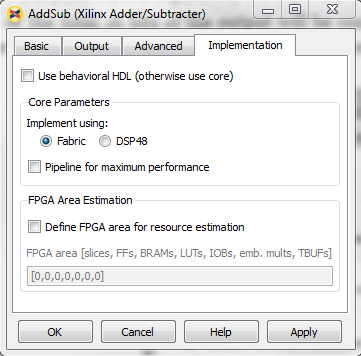
Figure 6
Registers
Next, we will add the set of registers at the output of the adder. Registers can be implemented using the “Delay” block found in the “Xilinx Blockset\Basic Elements” category. We will keep all the settings of this block as they are.
Connecting the “AddSub” block to the “Delay” block, we obtain the schematic shown in Figure 7.
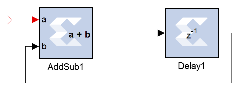
Figure 7
Quantizer
Now, we need to add the “Quantizer” of Figure 2 which passes the p most significant bits (MSBs) of the accumulator to the lookup table (LUT) and discards the other bits. This functionality can be achieved with the “Slice” block which is in the “Xilinx Blockset\Basic Elements” category. The symbol and the configurable parameters dialog box for a “Slice” is shown in Figure 8.
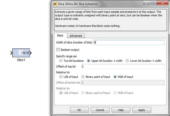
Figure 8
The parameter “Width of slice (number of bits)” specifies the number of bits to extract from the input. Assuming that eight MSBs of the accumulator output must be conveyed to the LUT, we know that the width of the output is eight, so we set the “Width of slice” to eight as shown in the figure.
We also need to specify which bit positions of the input are taken to form the eight-bit output of the “Slice” block. This can be done using the “Specify range as” parameter. There are three options for this parameter. We choose the “Upper bit location + width”. We should specify the location of the upper bit from the input that will be passed on to the MSB of the “Slice” output. Since we want the eight MSBs of the input, the upper bit will be the MSB of the input. Hence, we set the “Offset of top bit” to zero and “Relative to” to “MSB of input”. This means that the upper desired bit has zero offset relative to the MSB of the input. The width of the slice is already specified in the “Width of slice” parameter. Hence, the desired range of the input is fully specified. For more information about this block, refer to page 327 of this Xilinx document.
ROM
We will add a “ROM” from “Xilinx Blockset\memory” category. The symbol and the configurable parameters dialog box for a “ROM” is shown in Figure 9. Since the address input of the ROM is p=8 bits wide, we should set the “Depth” of the ROM to $$2^8=256$$ . As shown in the figure, we can easily write a mathematical expression to specify the content of the ROM. The mathematical expression in Figure 9 generates 256 samples from one period of a sinusoid. These samples will be taken based on the data precision that will be specified in the “Output” tab. You can also choose the memory type which can be implemented as either a “Distributed memory” or a “Block RAM”. We will use a Block RAM to implement the required memory.
The data format of the stored values can be chosen under the “Output” tab. We will use the default parameters as shown in Figure 10. Note that the “Arithmetic type” is “signed (2’s comp)” because our samples include negative values. From the total 16 bits of the output only two bits are allocated to the integer part because the maximum and minimum of the samples are +1 and -1, respectively. The remaining bits are used to represent the fractional value of the samples.
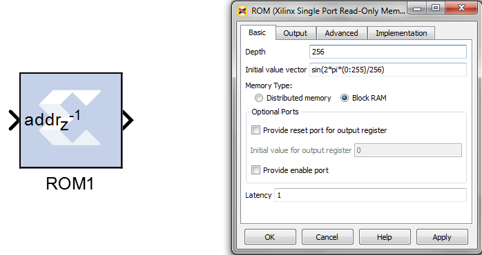
Figure 9
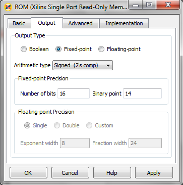
Figure 10
Data Type Conversion Between the Xilinx Portion and Simulink
Connecting the discussed blocks according to Figure 2, we obtain the schematic shown in Figure 11.
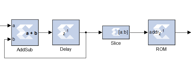
Figure 11
The model is almost complete but we need some other blocks to simulate the system. Unlike the Xilinx blockset which uses fixed-point numbers to represent different values; the Simulink environment has its own data type. For example, Simulink may employ the “double” data type which is a 64-bit two’s complement floating-point number. That’s why we need some blocks to perform data type conversion when transferring the data from Simulink to the Xilinx portion of Figure 11 or when transferring the output of Figure 11 to the Simulink environment. This can be achieved using the “Gateway In” and “Gateway Out” blocks as shown in Figure 12.
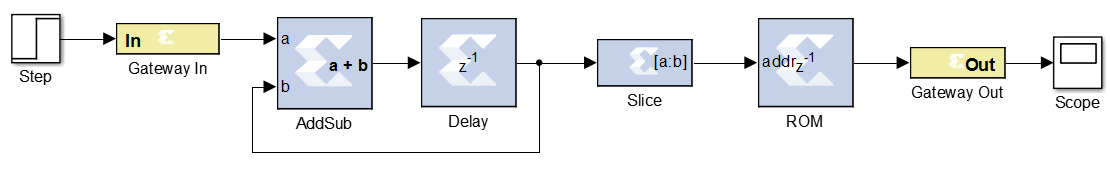
Figure 12
We’ll look at the parameters of the “Gateway In” and “Gateway Out” blocks in a minute but, before that, you should note that two other blocks, “Step” at the input and “Scope” at the output, are added to the model. As you can see, after adding the “Gateway In” and “Gateway Out” blocks, we can apply an input to our model using the Simulink general “Source” blocks. Or, we can monitor the outputs of the system by means of the Simulink general “Sink” blocks. In Figure 12, we have applied a “Step” to the phase increment input of the DDS. Also, the output of the ROM is monitored using a Simulink “Scope” block.
In addition to the data type conversion, the “Gateway In” and “Gateway Out” blocks define the top-level ports of the HDL design that will be later obtained from the Simulink model. For example, putting a “Gateway In” block before the “a” input of the adder, we let the system generator know that the “a” input is actually an input of the top-level design. Similarly, the “Gateway Out” defines the top-level outputs of the HDL design.
The configurable parameters dialog box for a “Gateway In” block is as shown in Figure 13.
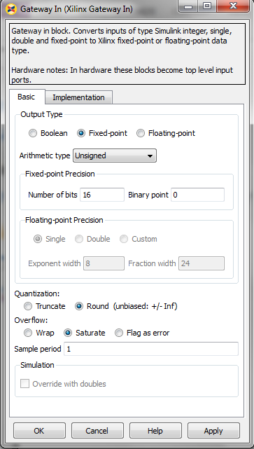
Figure 13
We should set the “Arithmetic type” to “Unsigned” and choose the “Number of bits” equal to 16 with no fractional bits, i.e. “Binary point”=0. Hence, any input from the Simulink environment will be represented as a 16-bit fixed-point unsigned number in the Xilinx portion of the design. Note that the format that we specified here is consistent with the data format of the Add/Sub block. We will leave the other parameters of the block as they are by default.
The “Gateway Out” block automatically detect the fixed-point format of its driving stage. That’s why, here, we can use the default settings of the block.
Xilinx System Generator Block
Any Simulink model that uses Xilinx blocks must include a “System Generator” block. This block allows us to control the system and simulation parameters. It also handles HDL code generation. The symbol and the dialog box for the “System Generator” block are shown in Figure 14.
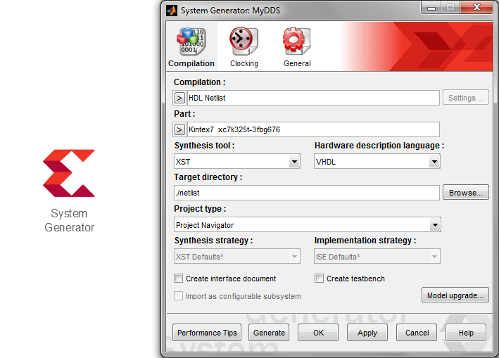
Figure 14
System Generator compiles the design into low-level representations. We can choose the type of the low-level representation from the “Compilation” parameter of the dialog box. In this article, we will choose “HDL Netlist” as shown in the figure. This generates a collection of HDL and some auxiliary files that can be processed by a synthesis tool. As you can see in the figure, we have chosen “XST” and “VHDL” as the synthesis tool and the HDL, respectively.
You should also choose the target device from the “Part” parameter of the dialog box and give the software the destination folder to store the generated files. Figure 15 below shows the “Clocking” tab of the dialog box.
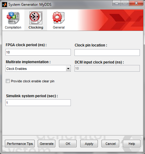
Figure 15
The first parameter “FPGA clock period (ns)” defines the period of the desired clock for the design. This parameter can be passed on to the synthesis tool in the next stages of the design. It can guide the synthesis software to choose an appropriate implementation based on the clock requirements of the design. In the above figure, the “FPGA clock period” is set to 10 nanoseconds. This means that we expect the design to be run with a clock period of 10ns on the board. Simulink can use a normalized form of this clock period in its simulations. This normalization is specified by the “Simulink system period (sec)” parameter of Figure 15. By setting this parameter to 1, every 10 ns of the hardware implementation will be represented by 1 second in the Simulink environment.
Simulation
To simulate the design, we set the “Step” input to go from 264 to 528 at “Step time” 500. You can use other arbitrary parameters for this block. Finally, we are ready to simulate our DDS model which is shown in Figure 16.
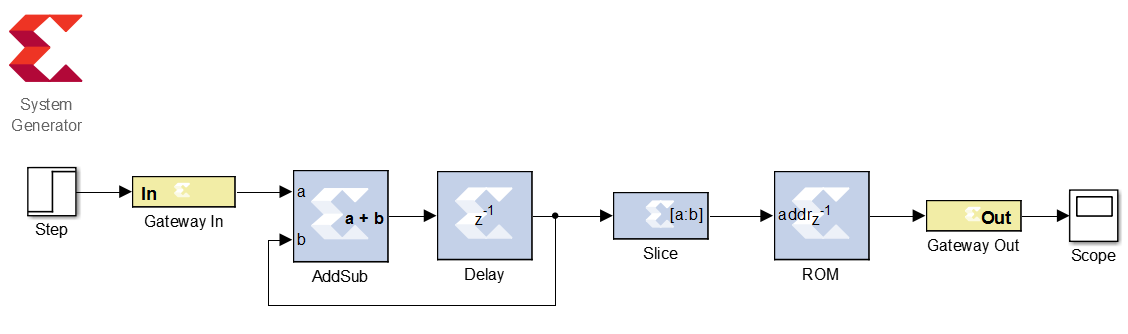
Figure 16
By clicking the “Run” button of Simulink, we get the following curve on the “Scope”.
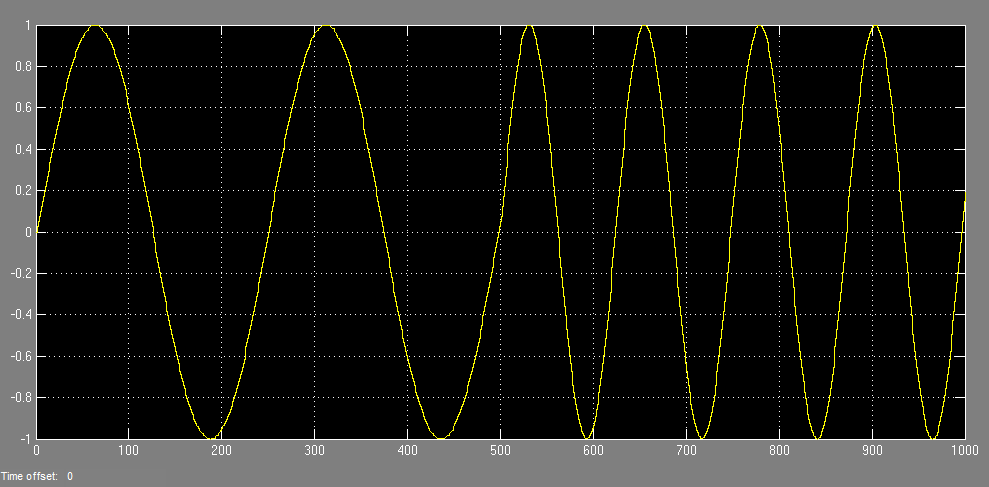
Figure 17
Since at “Step time”=500, the input goes from 264 to 528, the output frequency increases by a factor of two.
Adding the Design to an ISE Project
After setting all the parameters of the design, we can generate the VHDL description of the model by pushing the “Generate” button in Figure 14. This will produce a “.sgp” file which can be added to an ISE project.
By choosing “Add source” from an ISE project, we can include the .sgp file in our top-level design. Now, the added file can be used just the way we use an IP core. By clicking on the added file and choosing “View HDL Instantiation Template”, we can find the template to use the component.
To read about using IP cores and VHDL components, refer to Use the Xilinx CORDIC Core to Easily Generate Sine and Cosine Functions and How to Use VHDL Components to Create a Neat Hierarchical Design, respectively.
Conclusion
In this article, we used the “System Generator” to implement a simple DDS. The high-level graphical capabilities of Simulink allows us to easily model a complex digital system. After verifying the functionality of the design in the Simulink environment, we can generate the VHDL description of the design and add it to our project in the Xilinx ISE software.
To see a complete list of my articles, please visit this page.
Related Content


It would seem to work for me too, but how can I change the output frequency?
Thanks for the article. What’s the purpose of using the Quantization block?