Facebook
 Google
 GitHub
 Linkedin
Incomplete If Statements and Latch Inference in VHDL
In this article, we’ll see that a memory element can be unintentionally inferred from an incomplete “if” statement.
In this article, we’ll see that a memory element can be unintentionally inferred from an incomplete “if” statement.
In my previous article, Sequential VHDL: If and Case Statements, we looked at some examples of the “if” statement.
This article will focus on incomplete “if” statements. We’ll see that a memory element can be unintentionally inferred from either an incomplete “if” statement or incomplete signal assignments within an “if” statement. Finally, we’ll review an example application where we need to have D latches in our design.
“If” Statements without an “Else” Branch
“If” statements without an “else” branch can lead to undesired latch inference. Let’s see an example:
Example 1: Consider the following code:
1	library IEEE;
2	use IEEE.STD_LOGIC_1164.ALL;

3	entity Latch1 is
4	    Port ( d : in  STD_LOGIC;
5	           c : in  STD_LOGIC;
6	           q : out  STD_LOGIC);
7	end Latch1;

8	architecture Behavioral of Latch1 is

9	begin

10		process(d, c)
11		begin
12			if (c='1') then
13				q <= d;
14			end if;
15		end process;

16	end Behavioral;
This “if” statement is incomplete because it doesn’t have the “else” branch. According to this code, when the input c is high, the output, q, will be equal to the input d.
What if c is equal to zero? The code doesn’t explicitly specify the value of the output for this case. For c=‘0’, the previous value of the output will be held. This is equivalent to the memory effect that a D latch exhibits.
A latch is a level-sensitive memory element. As shown in Figure 1 (a), a basic positive-level D latch has three terminals: data input d, data output q, and a control input c. When the control input is high, the value of the data input is transferred to the data output terminal; when the control input is low, the output terminal will keep its last value. In contrast, the positive-edge D flip-flop (DFF), shown in Figure 1 (b), is transparent at the rising edge of clk; otherwise, the output retains its previous value.
Use of flip-flops is common in sequential circuit design, whereas latches are utilized only occasionally. The incomplete “if” statement of Example 1 is the standard code for implementing a D latch. That’s why the synthesis software doesn’t issue an error message for the above incomplete “if” statement. The designer must include an “else” branch to avoid the inference of a latch (unless of course a latch is desired).
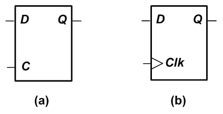
Figure 1. A positive-level D latch (a) and a positive-edge DFF (b).
The RTL schematic of the above code generated by the Xilinx ISE is shown in Figure 2. As you can see, there are some buffers along with an instance called ld. The ld instance in this figure represents a latch (see page 275 of the Xilinx Libraries Guide for Schematic Designs).
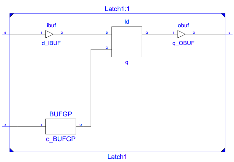
Figure 2
Example 2: Write VHDL code for a circuit that has an output, eq, and two two-bit inputs, a and b. The circuit compares the inputs; if a=b, the output, eq, is set to 1.
1	library IEEE;
2	use IEEE.STD_LOGIC_1164.ALL;

3	entity comp1 is
4	    Port ( a : in  STD_LOGIC_VECTOR(1 downto 0);
5		   b : in  STD_LOGIC_VECTOR(1 downto 0);
6		   eq : out  STD_LOGIC);
7	end comp1;

8	architecture Behavioral of comp1 is

9	begin

10		process(a, b)
11		begin
12			if (a=b) then
13				eq <= '1';
14			end if;
15		end process;

16	end Behavioral;
Once again, the “if” statement doesn’t have an “else” branch. Based on the discussion of the previous example, we can expect that this code will lead to a latch inference. An ISE simulation for this code is shown in Figure 3.

Figure 3
From 0 ns to 200 ns, the simulator cannot assign a value to the output eq; that’s why eq is uninitialized during this interval. From 200 ns to 300 ns, the two inputs are equal and eq is set to one. After 300 ns, although the inputs are no longer equal, the output eq remains high for the rest of the simulation. This shows a memory effect for eq in the simulation. The RTL schematic generated by ISE is shown in Figure 4.
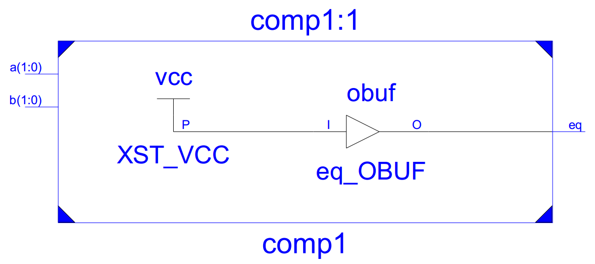
Figure 4
We can see that this VHDL code did not result in a properly designed circuit. Contrary to our expectations, latch inference did not occur. Instead, the output eq is simply connected to VCC through a buffer; in other words, the output is always logic high.
This example demonstrates the fact that an uninitialized value will be mapped to either logic high or low during synthesis. To achieve the intended operation, we can include the “else” branch and rewrite the above process as
Listing 1
	process(a, b)
	begin
		if (a=b) then
			eq <= '1';
		else
			eq <= ‘0’;
end if;
	end process;
The simulation of the new code is shown in Figure 5. As you can see, when the two inputs are equal, the eq output is one; when they are not equal, the output is zero.
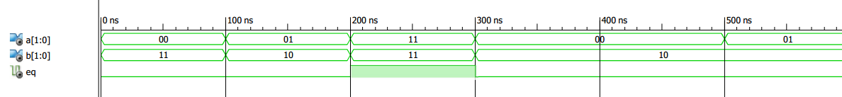
Figure 5
It is possible to avoid latch inference when using an “if” statement without an “else” branch. Remember that without an “else” branch, the last value of en is retained when the condition after the “if” keyword is false. By assigning a value to eq, before the “if” statement, we can avoid unintentional latch inference. In this case, the default assignment before the “if” statement will specify the value of eq when the “if” condition is false:
Listing 2
	process(a, b)
	begin
		eq <= '0';
		if (a=b) then
			eq <= '1';
		end if;
	end process;
The functionality implemented by Listing 2 is, in fact, equivalent to that of Listing 1.
“If” Statements with Incomplete Signal Assignment
Sometimes the “if” statement has the “else” branch but there are signals that don’t get a value under certain conditions. In this situation, the unassigned signals will retain their last value, and thus we can expect that incomplete signal assignment will lead to unintentional latch inference, just as the absence of an “else” statement does. For example, consider the following process:
	process(a, b, c)
	begin
		if (a=b) then
			ab_eq <= '1';
		elsif (a=c) then
			ac_eq <= ‘1’;
		else
			not_eq <= ‘1’;
		end if;
	end process;
The input a is compared with b and c and, based on the result of these two comparisons, the three outputs ab_eq, ac_eq, and not_eq may get a value. However, each branch of the “if” statement specifies the value of only one of the outputs. For example, when a=b, the output ab_eq will be set to one, but the other two outputs won’t get a value.
So, the above code will cause latch inference for the three outputs. To avoid latch inference, there are two possible solutions: we can either assign values to all three outputs in every branch of the “if” statement, or we can assign the outputs a default value before the “if” statement. The latter solution is used in the following code segment:
	process(a, b, c)
	Begin
		ab_eq <= ‘0’;
		ac_eq <= ‘0’;
		not_eq <= ‘0’;
		if (a=b) then
			ab_eq <= '1';
		elsif (a=c) then
			ac_eq <= ‘1’;
		else
			not_eq <= ‘1’;
		end if;
	end process;
Now that we are familiar with avoiding unintentional latch inference, let’s see an example where we actually want to have D latch elements in our design. A good example of a D latch application is a dual-edge flip-flop.
A Dual-Edge D Flip-Flop
Unlike a conventional D flip-flop which is sensitive to either the rising edge or the falling edge of the clock pulse, a dual-edge D flip-flop becomes transparent at both the rising and the falling edge of the clock. In other words, a dual-edge flip-flop stores data at both clock transitions.
You may think of some innovative coding options to implement such a flip-flop, but not all of these methods will function. (To read about some common mistakes in this regard, I'd recommend reading section 7.6 of Circuit Design and Simulation with VHDL.)
An appropriate method of creating a dual-edge flip-flop is to use two parallel latches in conjunction with a multiplexer. This technique is not necessary if you are using an FPGA that includes dual-edge flip-flops as part of its internal hardware.
The schematic is shown in Figure 6.
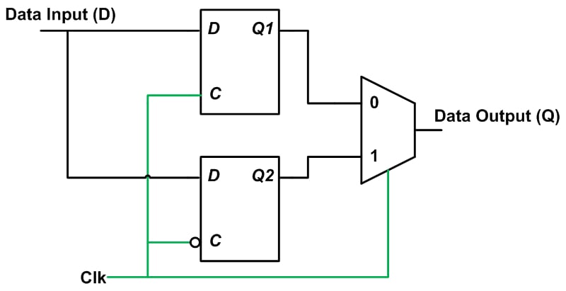
Figure 6
In this design, the upper D latch is a positive-level latch. It samples the value of the data input just before the falling edge of clk. The lower latch is a negative-level D latch that samples the data input just before the rising clk edge. If we apply the clock to both latches and to a multiplexer that selects between the outputs of the two latches, we can assign D to Q every time the clock transitions. A VHDL implementation would use code segments similar to that of Example 1 to generate the D latches (see Example 7.6 of this book for the complete VHDL description of a dual-edge DFF).
Summary
- “If” statements without an “else” branch can lead to undesired latch inference.
- A flip-flop is an edge-sensitive memory element, and a latch is level-sensitive.
- We can use a default assignment before the “if” statement to avoid unintentional latch inference, even when no “else” branch is included.
- Incomplete signal assignment within an “if” statement can lead to unintentional latch inference.
- A dual-edge D flip-flop becomes transparent at both the rising and the falling edge of the clock. If the target FPGA has only single-edge flip-flops, we can use two parallel latches along with a multiplexer to build a dual-edge flip-flop.
To see a complete list of my articles, please visit this page.