 Facebook
 Google
 GitHub
 Linkedin
The Operation and Characteristics of Voltage-Mode R-2R DACs
This article looks at the voltage-mode R-2R DAC structure.
This article looks at the voltage-mode R-2R DAC structure.
In this article, we'll take an exploratory look at what R-2R DACs are and how to implement them.
First, we'll briefly review a Kelvin divider DAC. Such structures are simple but they require a large number of resistors and switches to implement a high-resolution DAC. One solution to this problem is a DAC structure known as an R-2R DAC. These structures make clever use of a ladder network to implement a DAC with fewer resistors.
What Is a DAC?
A digital-to-analog converter (DAC) receives data represented as a digital code and produces an equivalent analog output (See Figure 1 below). It’s worthwhile to mention that, in addition to the digital input, DACs need an analog reference voltage or current to operate. This reference can be generated inside the DAC chip or provided externally.
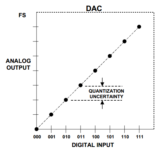
Figure 1. Image courtesy of Analog Devices.
The above ideal transfer function corresponds to a three-bit unipolar DAC. Note that both the DAC input and output are quantized values and the transfer function actually consists of eight points (rather than a line going through these eight points). Moreover, the maximum analog output (the output for an input code of all 1’s) is one step below the full-scale (FS) value.
Intro to the String DAC (Kelvin Divider): The Problem of 2n Resistors
A basic structure to produce the transfer function of Figure 1 is shown in Figure 2 below. Called a string DAC or a Kelvin divider, this structure uses eight equal resistors in series to produce the eight different voltage levels of a three-bit DAC. For example, to produce an analog output equal to VREF/4, we only need to turn the switch sw4 on.
The output buffer is used to prevent the resistor string from experiencing any loading effect from the DAC output node, VDAC.
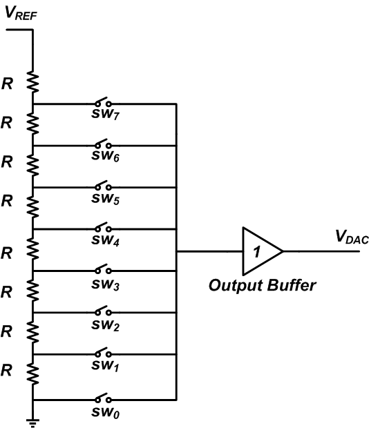
Figure 2
One major disadvantage of the Kelvin divider is that an n-bit DAC requires 2n resistors and switches. That’s why it’s not at all easy to use this method to build a high-resolution DAC (though one may combine a Kelvin divider with other techniques to build a more complex DAC).
There is an interesting method, however, that uses a ladder network to significantly reduce the number of resistors. These structures, called R-2R DACs, are discussed in the next section.
Analyzing an R-2R DAC Circuit
A basic four-bit R-2R voltage-mode DAC is shown in Figure 3. The digital code should be applied to the inputs D3...D0, where D3 is the most significant bit (MSb) and D0 is the least significant bit (LSb). Please refer to a previous article by Robert Keim to learn more about most/least significant bits/bytes and endianness.
As you can see, there are two different resistor values (R and 2R) in the ladder network.
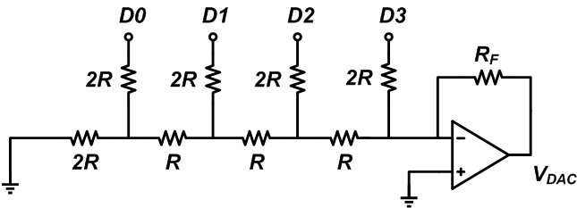
Figure 3
R-2R DAC Resistors
Some observations can make the analysis of the circuit simpler:
- Looking to the left of each R resistor, we’ll always see an equivalent resistor of R. This is shown by the blue arrows in Figure 4.
- Considering the previous observation, we know that looking from the right terminal of the R resistors, we’ll always see an equivalent resistor of 2R (red arrows in Figure 4).
Note that for calculating the equivalent resistors, the voltage sources applied to D3...D0 are shorted to ground.
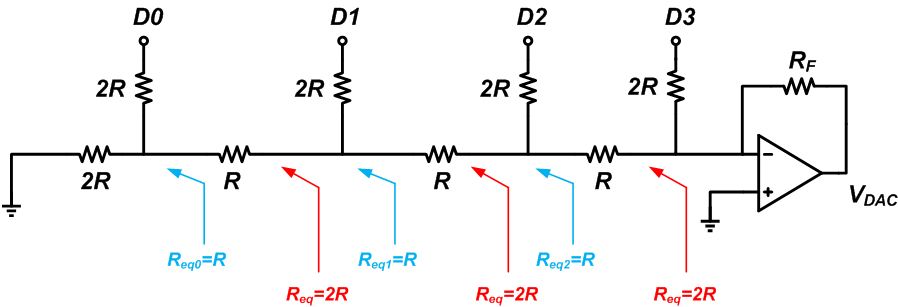
Figure 4
Circuit Operation
Now let’s examine the circuit operation. Assume that D0 is connected to VREF and the other bits are logic low; we obtain the circuit in Figure 5.
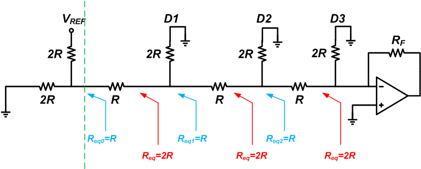
Figure 5
Applying the Thevenin theorem, we can model the circuitry to the left of the dashed line as shown in Figure 6.
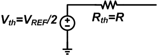
Figure 6
The Thevenin equivalent voltage is VREF divided by two, and the Thevenin equivalent resistance is equal to R.
Now, we use this equivalent circuit and obtain the circuit in Figure 7.
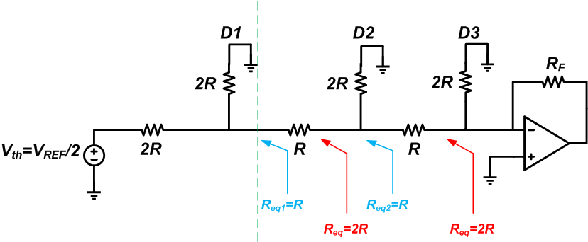
Figure 7
Simplifying an R-2R DAC Circuit with Thevenin's Equation
If we consider the circuit to the left of the dashed line in Figure 7, we observe a repeated pattern. There are two 2R resistors and a voltage source. The Thevenin equivalent of this part of the circuit will be as shown in Figure 8.
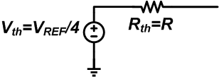
Figure 8
Hence, VREF is again reduced by a factor of two, and the equivalent resistance is still R. If we connect this model to the rest of the circuit, the previous pattern will appear again. This is shown in Figure 9.
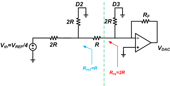
Figure 9
Considering our previous simplifications, we can easily find the Thevenin equivalent of the circuitry to the left of the dashed line. The Thevenin voltage will be VREF/8, and the Thevenin resistor will be 2R. Inserting the Thevenin equivalent, we obtain Figure 10.
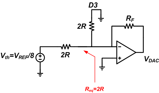
Figure 10
Considering the virtual ground at the inverting input of the op-amp, we can see that no current will flow through the resistor that leads to the grounded D3 input, and thus the current (VREF/8)/2R will flow through the feedback resistor (RF). Assuming RF=2R, the output voltage will be VDAC = -2R ✖ (VREF/8)/2R = -VREF/8. This output voltage corresponds to the DAC LSB.
Now, let’s examine other digital input combinations. Assume that D1 is connected to VREF and the other bits are logic low. Considering our first observation, we can model the circuit as shown in Figure 11.
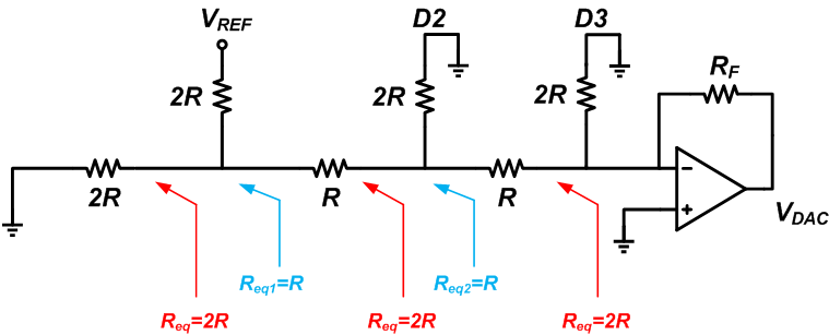
Figure 11
Applying the Thevenin theorem, we obtain the following schematic.
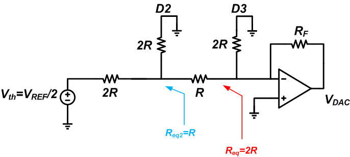
Figure 12
This is the same as Figure 9 except that the input is VREF/2 instead of VREF/4. Considering the result of the case D3D2D1D0 = 0001, if RF = 2R we obtain VDAC = -VREF/4.
If D2 is connected to VREF and the other three bits are logic low, we get the model in Figure 13.
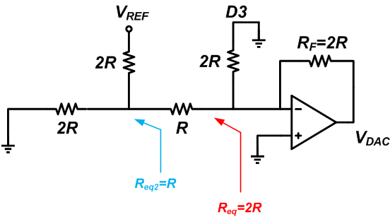
Figure 13
Applying Thevenin’s theorem, we obtain the circuit in Figure 14.
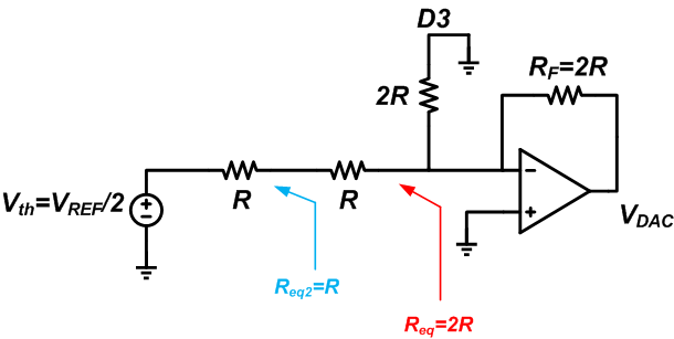
Figure 14
Considering the virtual ground at the inverting input of the op-amp, the current (VREF/2)/2R should flow through the feedback resistor. Hence, we have: VDAC = -VREF/2.
To examine the MSB, we assume that D3 is connected to VREF (logic high) and the other three bits are connected to ground (logic low). In this case, we obtain the model in Figure 15.
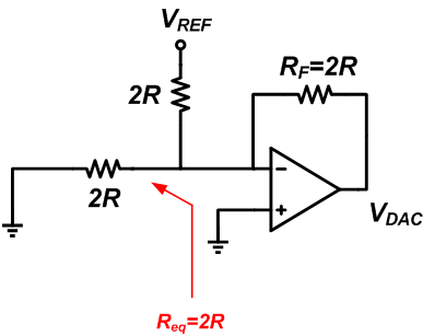
Figure 15
Hence, the output voltage will be VDAC = -(VREF/2R)✕2R = -VREF.
To summarize, connecting the inputs D3, D2, D1, and D0 to VREF can respectively produce voltage steps of -VREF, -VREF/2, -VREF/4, and -VREF/8. These voltage steps are the binary-weighted fractions of a reference voltage that are required when performing a digital-to-analog conversion. Since the circuit is linear, a combination of the inputs will produce the same combination of the corresponding output voltage steps. For example, if D0 and D1 are connected to VREF and D2 and D3 are logic low, the output will be -VREF/8 -VREF/4 = -3VREF/8. Note that the feedback resistor, RF, directly affects the gain of the DAC.
Some Important Characteristics of the Voltage-Mode R-2R DAC
The resistive connections in the R-2R ladder network are never disconnected by switches (as in the Kelvin divider). The design is such that the inverting terminal of the op-amp always sees a constant equivalent resistance no matter what digital code is applied to the DAC. In other words, the output impedance of the ladder network is constant. This makes stabilizing the amplifier or the unity-gain buffer easier.
However, the reference voltage source observes a varying load impedance from the ladder network. Hence, the reference generator should be able to produce an accurate voltage for a wide range of load resistance.
The input-to-output response of an R-2R DAC can be non-monotonic if there is a relatively large deviation from the ideal component values. A monotonic DAC response is either entirely nonincreasing or entirely nondecreasing. For example, the input-output characteristic of a Kelvin divider is monotonic. If we increase the input digital code, the output analog voltage will either increase or (in the worst-case scenario) retain its value; it will not decrease. Hence, a component mismatch cannot lead to a non-monotonic response.
This is not the case with an R-2R DAC. With the structure of Figure 4, the analog output should decrease with an increase in the input code. However, assume that, due to a mismatch in the resistor values, the output voltage step corresponding to the MSB is -3✕VREF/4 rather than the ideal value -VREF. If the input code changes from 0111 to 1000, the output will go from -VREF/2 - VREF/4 - VREF/8 = -7✕VREF/8 to -3✕VREF/4.
Therefore, if we have mismatch, an increase in the input code can lead to an increase in the analog output voltage, and thus the input-to-output response can be non-monotonic! Note that some applications require the use of a DAC in a closed-loop system. In these cases, a non-monotonic DAC response can change negative feedback to positive feedback. That’s why monotonicity can be important depending on the application.
In this article, we briefly reviewed a Kelvin divider DAC. Then, we examined a voltage-mode R-2R DAC. We saw that an R-2R structure makes clever use of a ladder network to significantly reduce the number of resistors, especially for a high-resolution D/A converter.
To see a complete list of my articles, please visit this page.
Related Content


Neat article. For the R-2R, the VREF would typically be Vcc/2 based on your circuit, right?
Thanks for the input! Using an ideal op-amp, I think we don’t have any limitation about the value of Vref but considering the real-world implementation, Vref should be chosen in a way that the op-amp circuitry could function correctly. For example, we have limitations for the common-mode voltage of the op-amp inputs. Such considerations can set upper and lower limits for the value of Vref.