Facebook
 Google
 GitHub
 Linkedin
What Is Inductance and How Does It Apply to Ground Bounce?
Why you should care about even small amounts of inductance.
Learn about the physics of current in a wire and why you should care about even small amounts of inductance.
PCB designers often pick up information from a variety of sources, including "off the mean streets and datasheets." To make good decisions, you need to understand the underlying physics and mechanical construction of your components. This article looks at inductance as it applies to ground bounce.
How Does Current Travel Down a Wire? A Review of Electromagnetics Physics
A wire with charges flowing randomly back and forth over short sections of its length will have no current and no measurable magnetic field. However, if a potential difference exists between two spots on that wire, charges in locations of high electrical potential energy will begin to migrate to locations of lower electrical potential energy, creating a current.
As the current increases from zero, some amount of energy will be transferred to and stored in a magnetic field that encircles the wire. As time increases, the changes in the electric field and magnetic field will propagate along and outward from the wire. These changes to the electric and magnetic fields occur at a fast but finite speed that is determined by the permittivity and permeability of the wire and its surroundings.
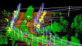
In the image below, a wire is shown (green/red cylinder) with accompanying magnetic fields shown in circular cross-sectional slices. The green/red color of the wire represents 0 V and 1 V potential.
When the left end of the wire transitions from 0 V to 1 V, charges begin to move to the right, generating a magnetic field that encircles the wire. As the wire transitions back to 0, the magnetic field dissipates.

This visual aid shows that transitions to electromagnetic fields take time to propagate. This is an artistic interpretation rather than a strict mathematical model by Mark Hughes.
While the current is constant, the magnetic field remains constant. If the current decreases, the magnetic field will decrease, but not before it puts up a fight.
The energy previously stored in the magnetic field is quickly converted to electrical energy in the form of a potential difference that induces a current to run along the length of the conductor. Over a period of time, the magnetic field energy and potential difference decay to zero.
The Role of Inductors
Inductors have the ability to create large instantaneous voltages, a property often exploited in boost voltage converters. If the current amplitude can be caused to change in a very short period of time, as is often the case during switching states, the generated potential difference will be significant, even if the inductance of the circuit is very low.
$$\triangle \text{V}=−L\frac{\text{dI}}{\text{dt}}$$
It just so happens that modern integrated circuits are designed with very low rise and fall times (<10-9 s), have multiple output pins that share the same Vss and Gnd lines (which increases current during simultaneous switching), and have very small noise-margins. That means that we need to be concerned with even very small amounts of inductance.
During switching, the induced voltages can cause an ICs Gnd and Vss potentials to be significantly different than the Gnd and Vss potential of the rest of the circuit.
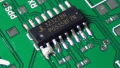
Package Inductance
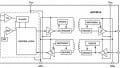
Inside an IC package is a small die. Pads on the die connect to external package pins with thin bonding wires. Those wires have a small, but non-trivial amount of inductance associated with them. Short switching intervals, combined with the package inductance (mostly attributed to the bonding wires), can cause significant voltages to be generated between the pins of packages and the semiconductors on the IC die.
Most PCB designers have no control over package construction, but they can sometimes select smaller packages or flip-chip packages in their designs—a QFN package will almost certainly have lower package inductance than a DIP package containing the same die.

Inside every IC package is a die that is physically connected to the pins of the IC package, typically with bonding wires.
Trace Inductance
Unlike package inductance, you can manipulate your PCB design to decrease or increase the inductance of your circuit. Take measures to decrease inductance whenever possible. Do this by providing immediate, uninterrupted return paths for all of your signal lines, provide ground return vias near your signal vias, and provide uninterrupted ground planes on adjacent layers. For more information, see this TI app-note.

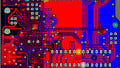
This 3D cross-section and top-view of a fictitious circuit shows the current path in the vertical and horizontal orientation through an arbitrary component. All changing signal lines will find a return path to the source.
Circuits store recoverable energy in the electromagnetic fields that surround their traces. When that field energy is converted back to a potential difference inside your circuit, it can disrupt the logic states and cause your circuit to behave unpredictably. Take a moment to read this article on ground-bounce to learn more.
Related Content