Facebook
 Google
 GitHub
 Linkedin
CMOS Bandgap References
Let's face it: a bandgap reference is a bipolar concept. It needs a diode and the difference between two diodes. And the only diodes good enough are diode-connected bipolar transistors (or, in some designs, the base-emitter diodes of bipolar transistors).
Transistors in CMOS Processes
Fortunately, there are some layers in a CMOS integrated circuit that, although not intended for this purpose, can be used to make a passable bipolar transistor. The most obvious ones are those used for a P-channel transistor:
- The P-type region (PMOS source and drain) forms the emitter.
- The surrounding N-well forms the base.
- The P-type substrate forms the collector.
Such a vertical PNP device has limitations. For one thing, the collector is permanently tied to the lowest supply voltage. There’s no flexibility there at all.
Furthermore, the gain (hFE) is very low—about seven. In a bipolar process, we rely on a high gain (at least 100) to effectively eliminate the base resistance as a source of error.
So we will need to make the CMOS substrate PNP transistor large if we want reasonable gain— which we probably want to do anyway to get reasonable accuracy.
It’s also possible to make lateral PNP transistors in CMOS by using the P-channel drain/source diffusions as both the emitter and the collector. Such devices have a reasonable gain (100 or so).
However, unlike the substrate devices, they’re hardly ever characterized by the foundry. That means you can't consider lateral PNP transistors unless you want to spring for a rather expensive evaluation run. For that reason, we’ll consider only a CMOS bandgap reference using substrate PNP transistors here.
Designing a CMOS Bandgap Reference Circuit
Figure 9-22 is an example of a CMOS bandgap reference using vertical PNP transistors.
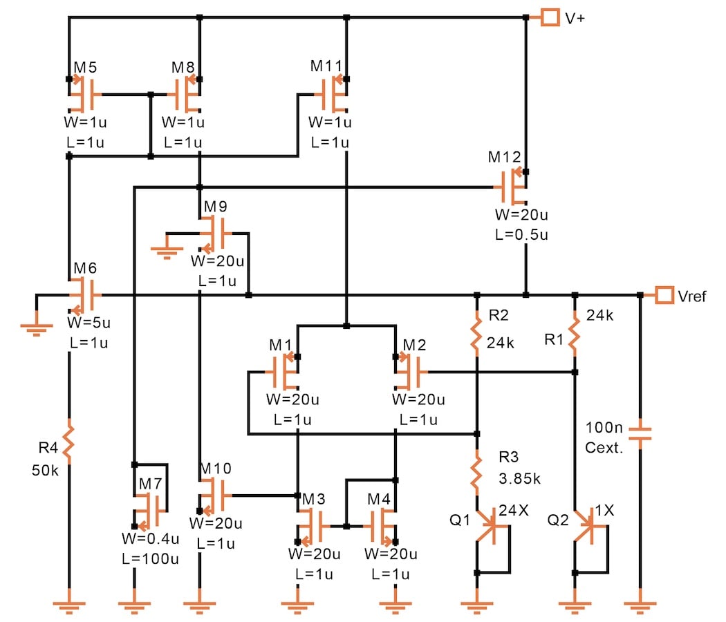
Figure 9-22. CMOS bandgap reference using PNP substrate diodes. [click to enlarge]
In the above figure, Q2 has a single 10 μm × 10 μm emitter. Q1 has 24 of them. For improved matching, Q2 is usually placed in the center of the layout and then surrounded by two rows and columns of identical Q1 devices. Compared to 0.12 μm, 0.18 μm, or even 0.35 μm CMOS devices, this circuit is very large (get used to it!).
R1 and R2 are equal so that the ΔVBE appears across R3. The error voltage is amplified by M1, M2, M3, M4, M10 and M12. These devices need to be as large as indicated in the figure.
For M1, M2, M3, and M4, the prime requirement is matching, which gradually improves as the area—the channel length times its width—is increased. Keep in mind that we’re working down at a level of one ΔVBE, which here amounts to about 82 mV.
For M10 and M12, the width needs to be substantial to get sufficient gain (transconductance). An increased length helps to reduce the influence of power supply variations. A cascode stage (M9) has been added to reduce it even more.
M7, which is a narrow and very long transistor, starts the circuit by feeding a small current into the loop. Once sufficient voltage appears at Vref, M6 and R4 take over and supply the operating current. This current is mirrored by M5, M6, and M11.
M12 is a P-channel transistor, which means that it provides a low minimum supply voltage (1.5 V). However, it makes frequency compensation difficult. The only practical way to do this is with an external capacitor, though placing it at the output also provides a good power supply rejection (–60 dB). The output impedance is 0.5 Ω up to about 1 mA.
With the transistors sized as shown and the resistors 4 μm wide, you can expect a production variation of ± 1.8% over a temperature range of 0 to 100 °C.
A word of caution: A bandgap reference is the ultimate test of accuracy for device models. For example, it’s very difficult to measure VBE over temperature accurately enough on a wafer for it to predict the behavior of a bandgap reference. With most CMOS processes, you need to make a bandgap reference to verify the models.