Facebook
 Google
 GitHub
 Linkedin
Low-Voltage Bandgap References
All of the bandgap references we’ve examined so far in this chapter have been built on the following principles:
- Add two circuit elements with equal but opposite temperature coefficients, so that their sum has a temperature coefficient of zero.
- One of the circuit elements is a diode with a voltage drop of about 600 mV.
- The second circuit element generates a multiple of ΔVBE that also amounts to about 600 mV.
With these designs, the minimum reference voltage (Vref) possible is, therefore, about 1.2 V.
Let’s now examine other approaches that avoid the addition and allow lower voltage operation.
A 1 V Bandgap Reference
The circuit in Figure 9-20 is another from the fertile mind of Bob Widlar. As early as 1978, he suggested this circuit that works with a 1 V supply—allowing operation from a single battery.
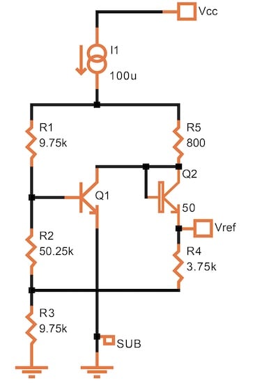
Figure 9-20. A 200 mV bandgap voltage reference designed by Widlar.
First off, he uses just about the largest emitter ratio practical, 50:1 between Q2 and Q1. This gives us a ΔVBE of about 100 mV at room temperature.
The VBE appears at the base of Q1 to ground. Because of that, the voltage at the entrance of the current source is higher by a fraction of VBE.
If we assume R5 to be zero, the voltage at Vref is that fraction of a VBE plus the ΔVBE of the 50:1 ratio in emitters of Q2 and Q1. If the value of R1 is such that the fraction of the VBE amounts to about 100 mV, then we have a temperature-stable Vref of 200 mV.
R5 provides some compensation for changes in I1. Also, connecting R4 to a tap at R2/R3 rather than ground creates a minor amount of second-order temperature compensation.
A Vref of 200 mV is just about the maximum value you can get from this design. Even with a much larger emitter ratio—say, 200:1—ΔVBE only amounts to 138 mV. Vref would then be about 272 mV.
A Two Current Bandgap Voltage Reference
The second approach we’ll discuss is considerably more complex but has greater flexibility. Two currents are created, one with a positive temperature coefficient and the other with a negative temperature coefficient. Summed, they produce a voltage drop in a resistor with a near-zero temperature coefficient. This concept is illustrated in Figure 9-21.
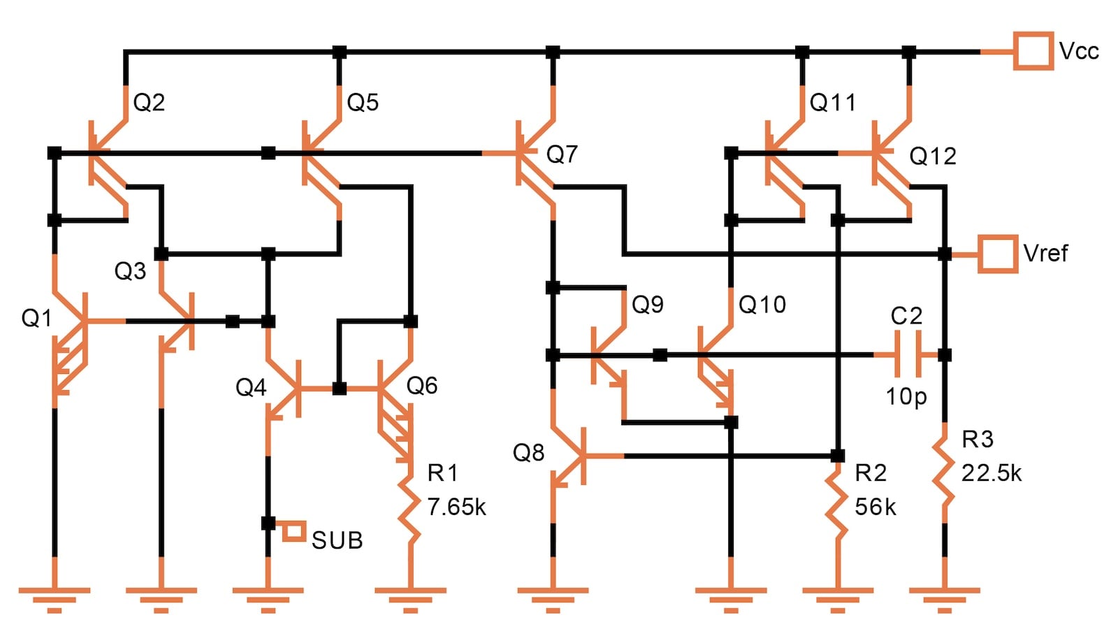
Figure 9-21. Bandgap reference with a minimum supply voltage of 0.9 V. [click to enlarge]
In the circuit above, two currents feed R3 to create the output voltage, Vref. As we will see, a positive temperature coefficient current from Q7 is countered by a negative temperature coefficient current from Q12.
The Positive Temperature Coefficient Current Source
The first current depends on the 3:1 emitter ratio of Q6/Q4 and the fact that Q4 is biased at twice the current of Q6. The effective emitter ratio is, therefore, 6:1. The current is determined by the ΔVBE, which is 47 mV at room temperature, and R1.
The feedback loop has a gain of three, carefully controlled by the 3:1 emitter ratio of Q1/Q3. In this way, the loop is frequency-compensated by the device capacitances. The loop is self-starting due to the leakage currents. The collector currents of Q2 and Q5 have a positive temperature coefficient.
Two identical currents are derived from Q7. One current feeds the output resistor R3. The other starts the second current source.
The Negative Temperature Coefficient Current Source
The second current depends on the VBE of Q8 and the value of R2. Again, the loop has a limited and well-controlled gain (the emitter ratio of Q10/Q9 and the 2:1 collector ratio at Q11/Q12). However, a small frequency compensation capacitor is still required.
The collector currents of Q11 and Q12 have a negative temperature coefficient. One collector of Q12 feeds the output resistor R3.
Operation of the Two Current Bandgap Reference
The sum of the two currents from Q7 and Q12 flowing through R3 causes a voltage drop of 250 mV, with a temperature coefficient near zero.
The two currents can be adjusted independently by changing the values of R1 and R2. This allows for fine-tuning of the temperature coefficient. The magnitude of the output voltage can be selected with the value of R3 without affecting the temperature coefficient.
Note that the currents depend on the resistor values. Though they’ll vary in production, R3 tracks these variations. The output voltage depends only on resistor matching.
The circuit’s output impedance is that of R3. Unless the load draws only a very small current, you’ll need to add an output buffer.
This bandgap reference works down to 0.9 V supply. The change in output voltage from 1 V supply to 1.5 V is 0.25%. Power supply rejection is –55 dB up to 10 kHz. To keep the power supply noise low at higher frequencies, you’ll need an external capacitor (10 nF) at the output.
Production variation is ± 3.6% from 0 to 100 ºC. This illustrates that the lower the supply voltage, the more difficult it is to achieve high performance—even if a more elaborate circuit is used.